Discover 169 technologies from leading innovators around the world.

NVIDIA NVLink is a high-bandwidth GPU-to-GPU interconnect and rack-scale fabric for AI training and inference. Distinct from NVLink-C2C chip-to-chip packaging links.
AI & HPCData CenterView Technology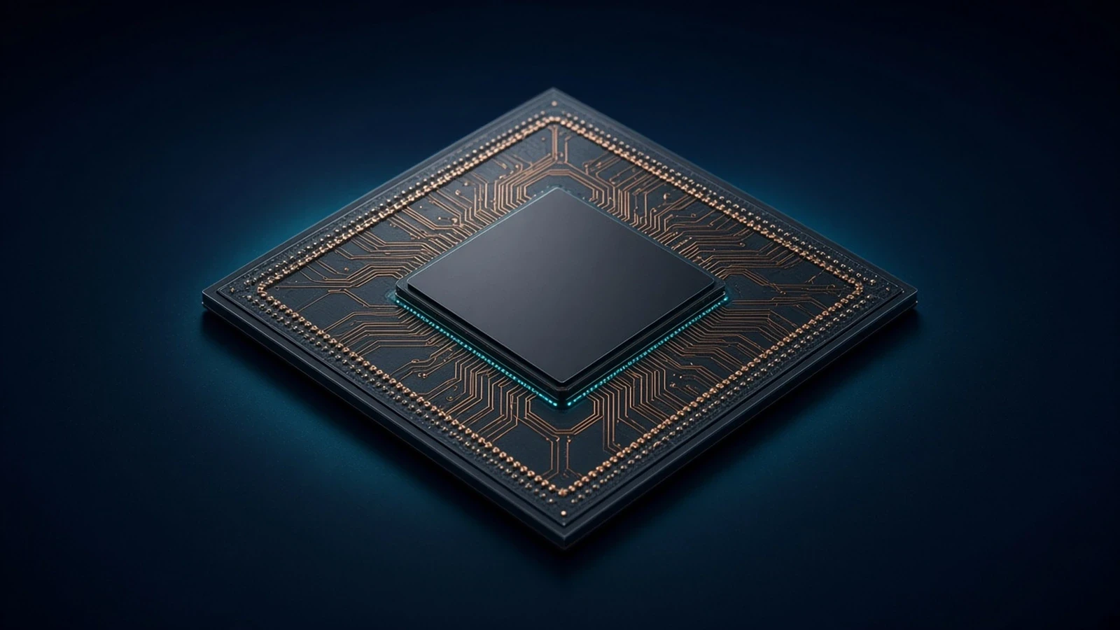
TSMC InFO is a wafer-level integrated fan-out packaging platform using high-density redistribution layers for mobile, network and high-performance computing integration.
AI & HPCConsumer ElectronicsTelecommunicationsView Technology
ASML TWINSCAN NXE is the 0.33 numerical-aperture EUV lithography platform used in high-volume manufacturing of advanced logic and memory chips. Distinct from High-NA EXE systems.
AI & HPCConsumer ElectronicsView Technology
Intel EMIB is a 2.5D packaging technology that embeds a silicon interconnect bridge in the package substrate to connect neighboring dies without a full-size interposer.
AI & HPCData CenterView Technology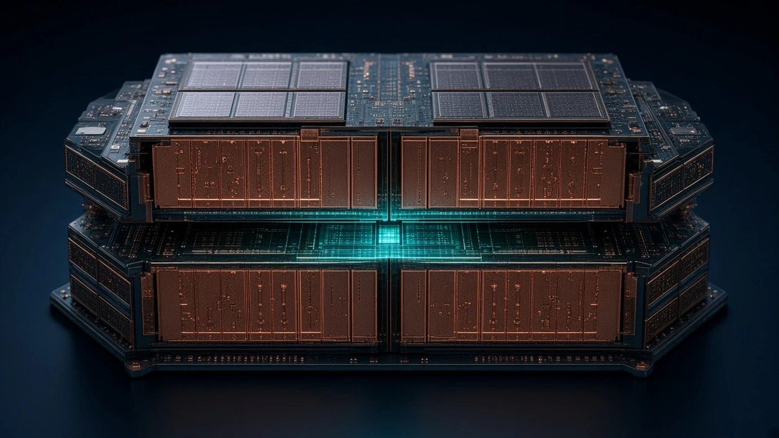
TSMC-SoIC is a wafer-level frontend 3D chip-stacking platform for homogeneous and heterogeneous chiplets, distinct from CoWoS 2.5D packaging and InFO fan-out.
AI & HPCData CenterView Technology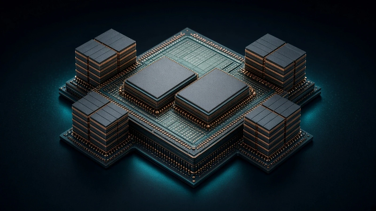
TSMC CoWoS is a 2.5D advanced packaging platform that integrates logic dies and high-bandwidth memory on an interposer for high-performance computing and AI systems.
AI & HPCData CenterView Technology
Morphing Machines REDEFINE is a many-core processor architecture that instantiates domain-specific compute structures on a shared fabric at runtime.
AutomotiveAI & HPCTelecommunicationsView Technology
FermionIC publishes multi-protocol SERDES semiconductor IP for high-speed chip-to-chip and system connectivity across advanced digital interfaces.
AI & HPCData CenterTelecommunicationsView Technology
Netrasemi NETRA A2000 is a mid-range edge AI system-on-chip for on-device machine-learning, vision and signal-processing workloads in embedded systems.
AutomotiveAI & HPCIndustrial+1View Technology
InCore publishes configurable RISC-V processor IP through an automated Core-hub generator that produces synthesizable core instances for custom semiconductor systems.
AI & HPCIndustrialIoTView Technology
Lightmatter Passage is a photonic interconnect platform using integrated photonics and three-dimensional connectivity approaches to scale high-bandwidth communication across advanced AI and computing systems.
AI & HPCData CenterView Technology
proteanTecs combines embedded on-chip monitoring agents and sensors with integration tools and analytics software to provide visibility into silicon performance, reliability and behavior across production and in-field operation.
AutomotiveAI & HPCData Center+1
Ayar Labs TeraPHY is an optical I/O chiplet that combines silicon photonics with CMOS technology to provide high-bandwidth, low-latency chip-to-chip and package-to-package connectivity for large-scale computing systems.
AI & HPCData CenterTelecommunicationsView Technology
Arm Chiplet System Architecture provides standardized system partitioning and connectivity foundations for reusable chiplet-based designs. It is an architecture, not a processor-core catalog.
AutomotiveAI & HPCData CenterView Technology
ASM Atomic Layer Deposition technology enables highly controlled, layer-by-layer deposition of ultrathin conformal films for advanced semiconductor logic, memory and packaging structures.
AI & HPCData CenterConsumer ElectronicsView Technology
NVIDIA NVLink-C2C is a high-bandwidth coherent chip-to-chip interconnect for processors, accelerators and custom silicon inside a package. Distinct from NVLink GPU-to-GPU fabric.
AI & HPCData CenterView Technology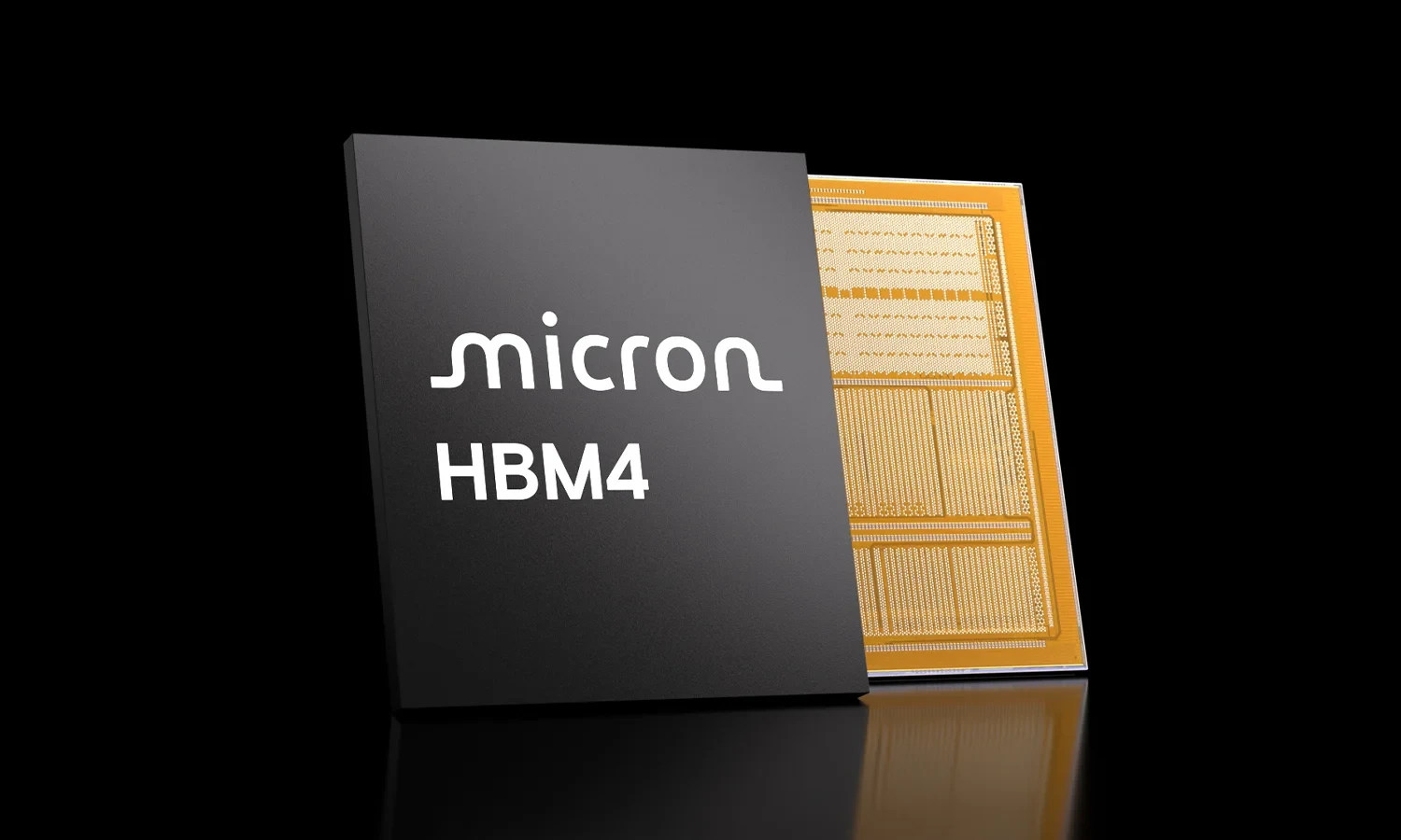
Micron high-bandwidth memory technology uses vertically stacked DRAM dies and high-density interconnects to provide high memory bandwidth and power efficiency for AI and data-center computing platforms.
AI & HPCData CenterView Technology
Cadence design platform for planning, implementing and analyzing 2.5D and 3D multi-die / chiplet systems.
AutomotiveAI & HPCData CenterView Technology
Synopsys die-to-die IP solution for Universal Chiplet Interconnect Express, including controller, PHY and verification IP.
AutomotiveAI & HPCData CenterView Technology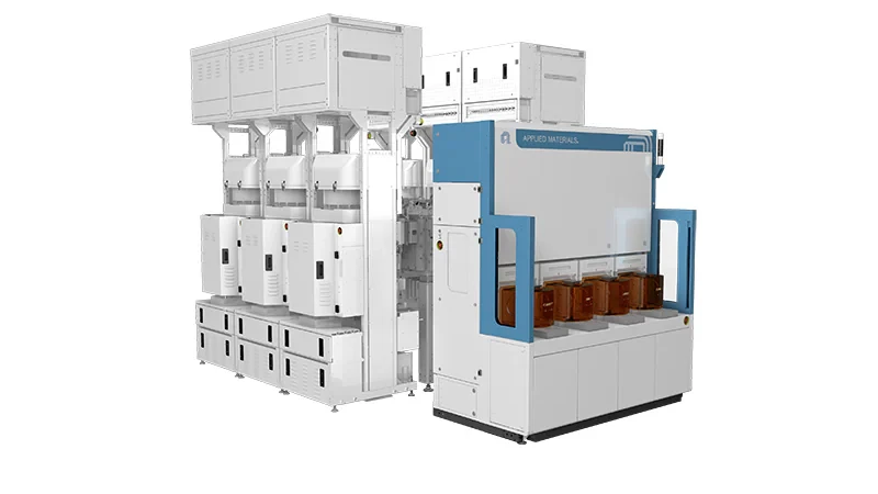
Modular semiconductor wafer-manufacturing chassis from Applied Materials for combining multiple chamber types on one system. Distinct from the Endura metallization platform.
AI & HPCData CenterView Technology
ASML High-NA EUV lithography platform (TWINSCAN EXE) using 0.55 numerical aperture optics. Distinct from 0.33 NA TWINSCAN NXE EUV systems.
AI & HPCConsumer ElectronicsView Technology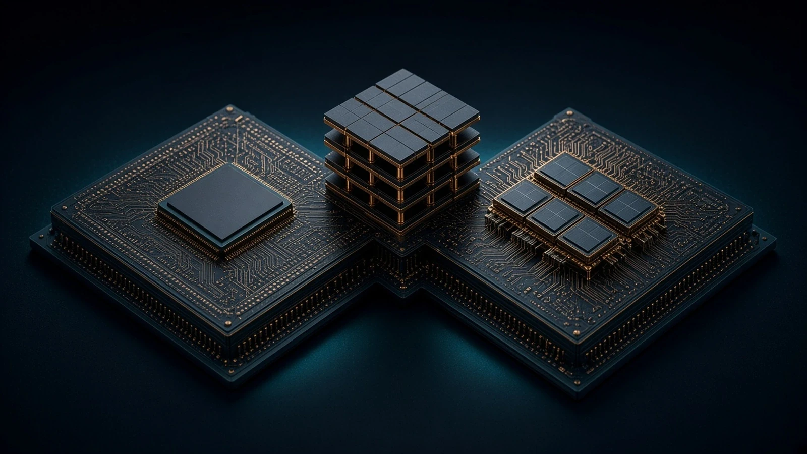
TSMC umbrella family of 3D silicon stacking and advanced packaging. CoWoS, TSMC-SoIC and InFO are constituent platforms listed separately.
AI & HPCData CenterView Technology
Intel Foundry 3D stacking and 2.5D chiplet packaging family, including hybrid-bonding options described as Foveros Direct 3D. EMIB is a separate 2.5D bridge platform.
AI & HPCData CenterConsumer ElectronicsView Technology