Discover 169 technologies from leading innovators around the world.
BlueField is NVIDIA’s data processing unit: Arm cores, high-speed Ethernet/InfiniBand and hardware accelerators for networking, storage and security offload, isolated from the host CPU.
AI & HPCData CenterTelecommunicationsView Technology
Oryon is Qualcomm’s custom 64-bit CPU microarchitecture, including cache hierarchy, branch prediction, prefetch and later Flex Cache, designed in-house and scaled across Snapdragon platforms.
AutomotiveAI & HPCData Center+1View Technology
TPU7x (Ironwood) is Google Cloud's seventh-generation TPU, built for large-scale training and inference.
AI & HPCData CenterView Technology
Micron DDR DRAM is a synchronous DRAM component family spanning successive double-data-rate generations for data-center, industrial and automotive designs.
AutomotiveData CenterIndustrialView Technology
Micron 3D NAND is a vertically stacked NAND flash technology family used as the semiconductor storage building block in data-center, client, mobile and automotive designs.
AutomotiveAI & HPCData Center+1View Technology
Micron LPDDR is a low-power DRAM family for mobile, client, automotive and data-center designs that need high bandwidth at reduced power. LPDDR generations remain one technology line.
AutomotiveAI & HPCData Center+1View Technology
Lam Research SABRE is an electrochemical copper-deposition platform for damascene interconnect, including logic, memory and high-bandwidth memory wiring. Distinct from Lam’s broader etch category.
AI & HPCData CenterView Technology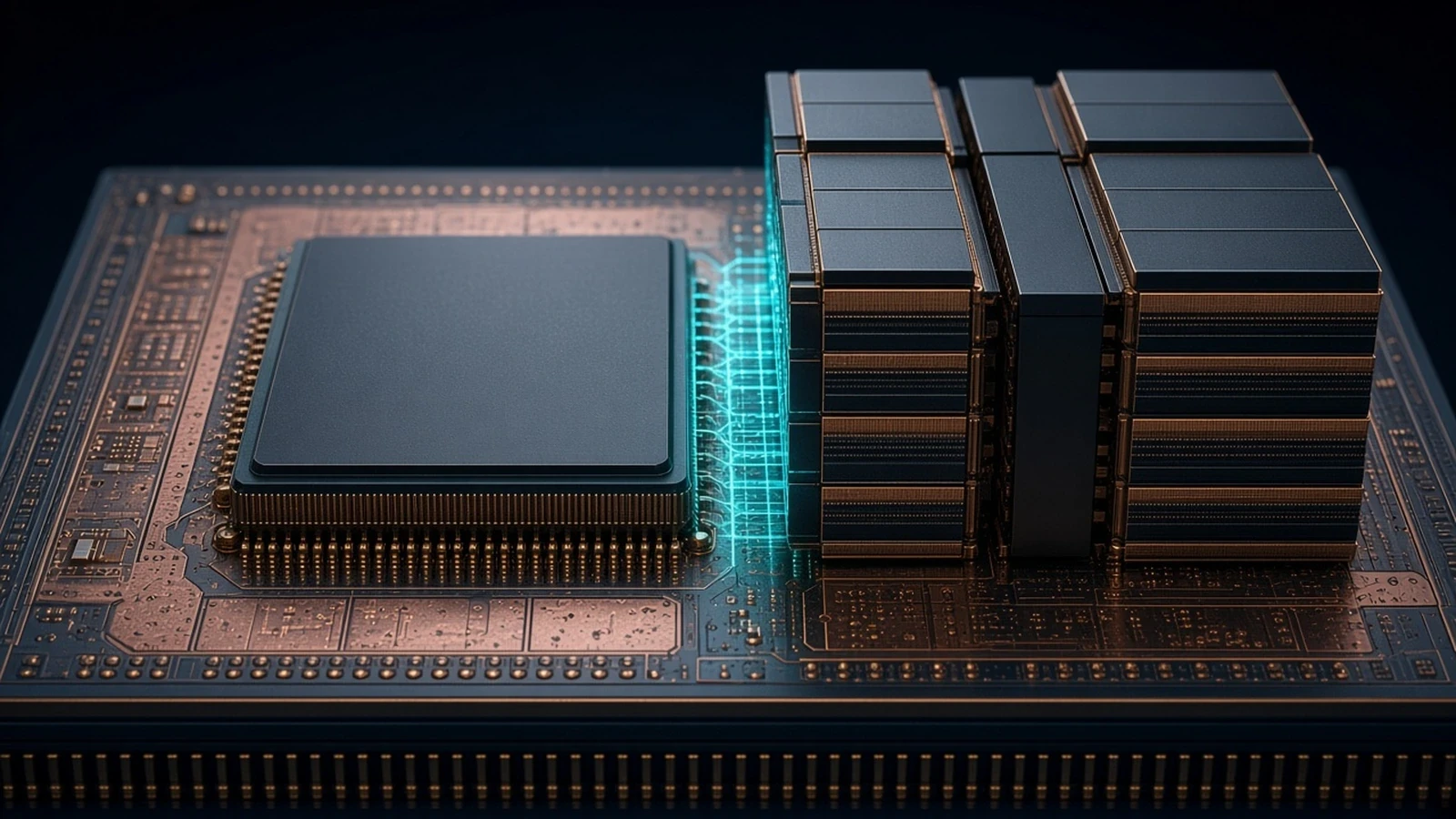
Synopsys HBM interface IP is a high-bandwidth memory interface family including controller, PHY and verification IP for AI and high-performance computing SoCs. Distinct from UCIe die-to-die IP.
AI & HPCData CenterView Technology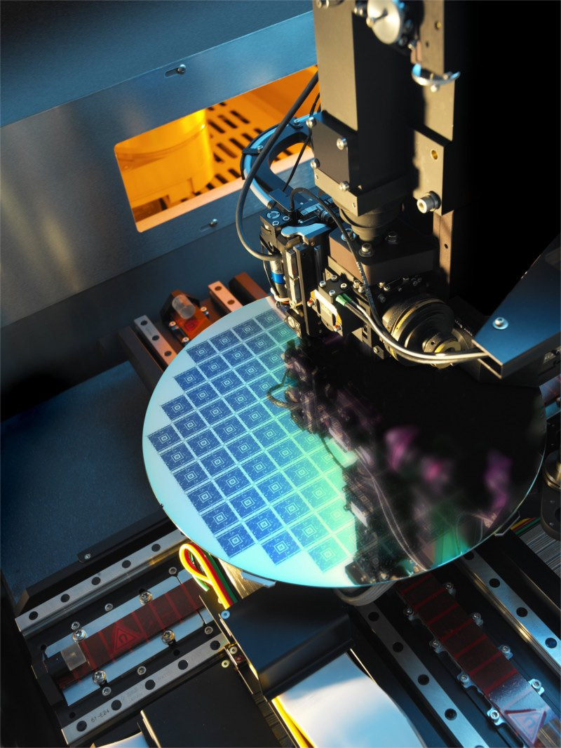
KLA overlay and dimensional metrology systems measure layer-to-layer alignment, critical dimensions and related pattern geometry. Distinct from defect inspection and review.
AutomotiveData CenterConsumer ElectronicsView Technology
Applied Materials Endura is an ultra-high-vacuum metallization platform used for physical vapor deposition and integrated multi-chamber sequences. Distinct from the Vistara wafer-manufacturing chassis.
AI & HPCData CenterView Technology
NVIDIA NVLink is a high-bandwidth GPU-to-GPU interconnect and rack-scale fabric for AI training and inference. Distinct from NVLink-C2C chip-to-chip packaging links.
AI & HPCData CenterView Technology
Intel EMIB is a 2.5D packaging technology that embeds a silicon interconnect bridge in the package substrate to connect neighboring dies without a full-size interposer.
AI & HPCData CenterView Technology
Lightmatter Passage is a photonic interconnect platform using integrated photonics and three-dimensional connectivity approaches to scale high-bandwidth communication across advanced AI and computing systems.
AI & HPCData CenterView Technology
Ayar Labs TeraPHY is an optical I/O chiplet that combines silicon photonics with CMOS technology to provide high-bandwidth, low-latency chip-to-chip and package-to-package connectivity for large-scale computing systems.
AI & HPCData CenterTelecommunicationsView Technology
NVIDIA NVLink-C2C is a high-bandwidth coherent chip-to-chip interconnect for processors, accelerators and custom silicon inside a package. Distinct from NVLink GPU-to-GPU fabric.
AI & HPCData CenterView Technology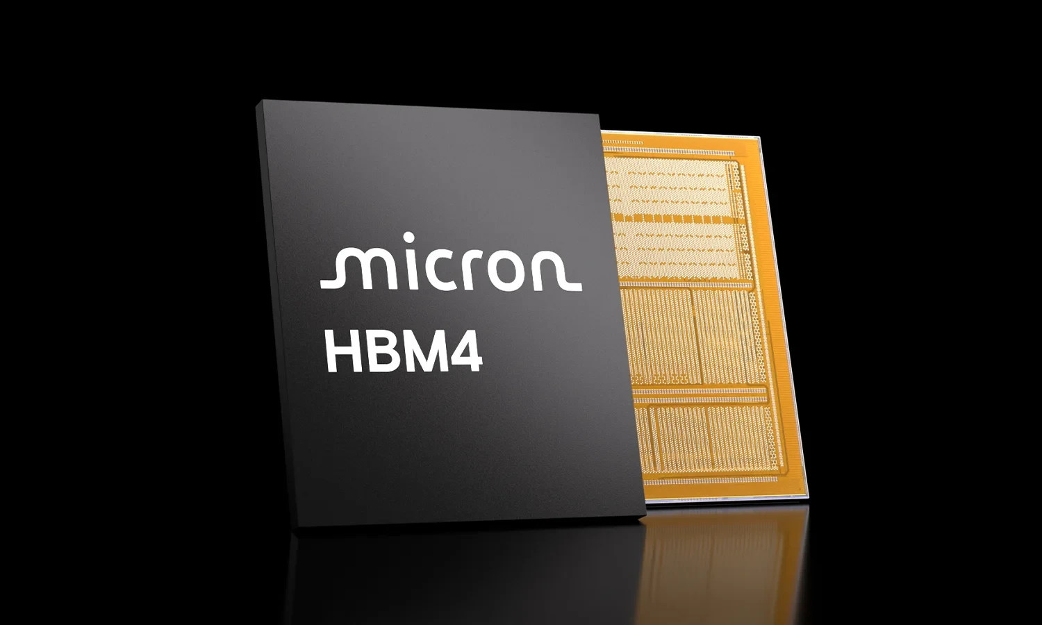
Micron high-bandwidth memory technology uses vertically stacked DRAM dies and high-density interconnects to provide high memory bandwidth and power efficiency for AI and data-center computing platforms.
AI & HPCData CenterView Technology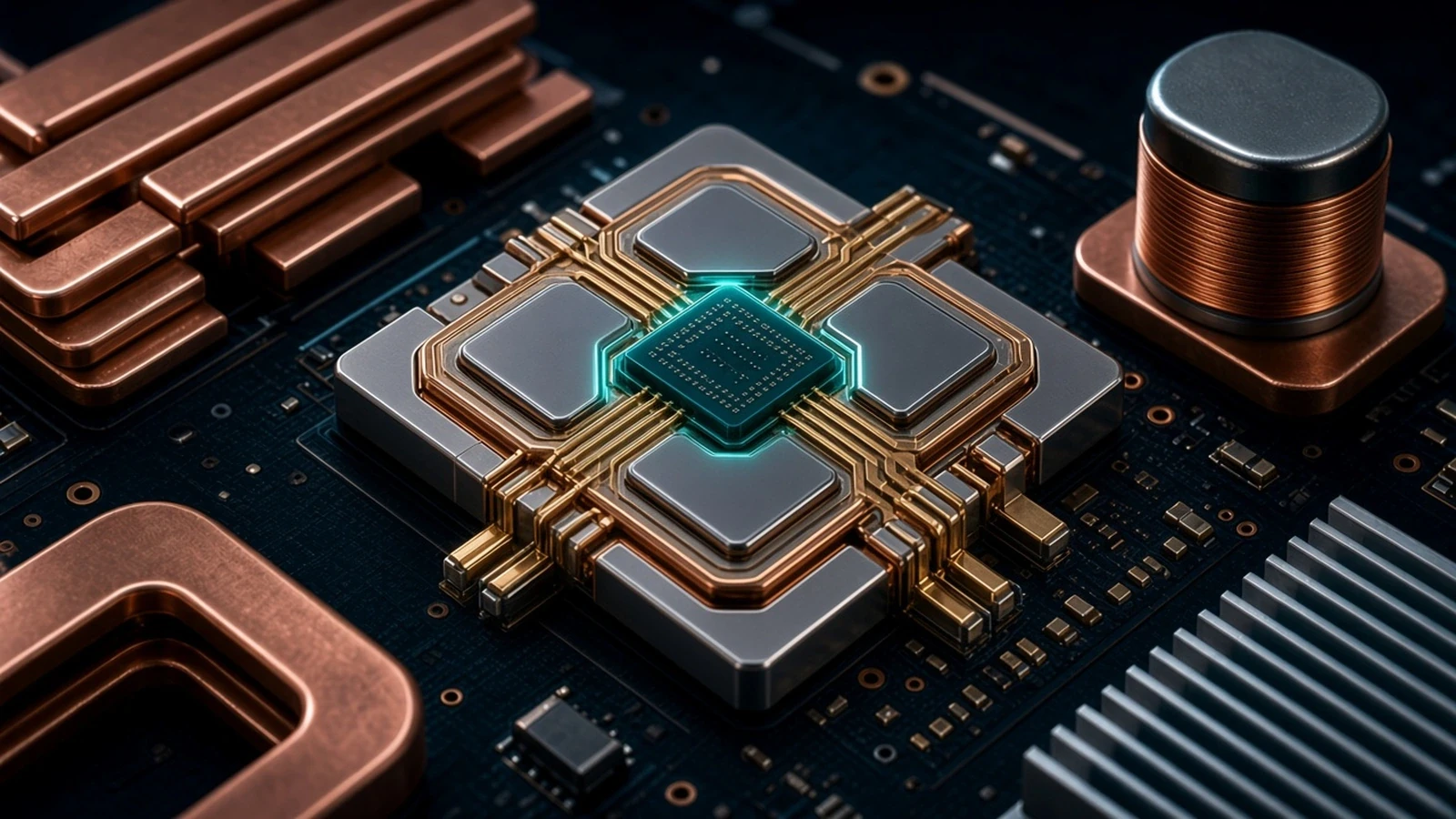
Microchip mSiC is a silicon carbide power semiconductor technology family spanning MOSFETs, Schottky barrier diodes, bare die and power modules. Those form factors are not separate listings.
AutomotiveData CenterIndustrial+2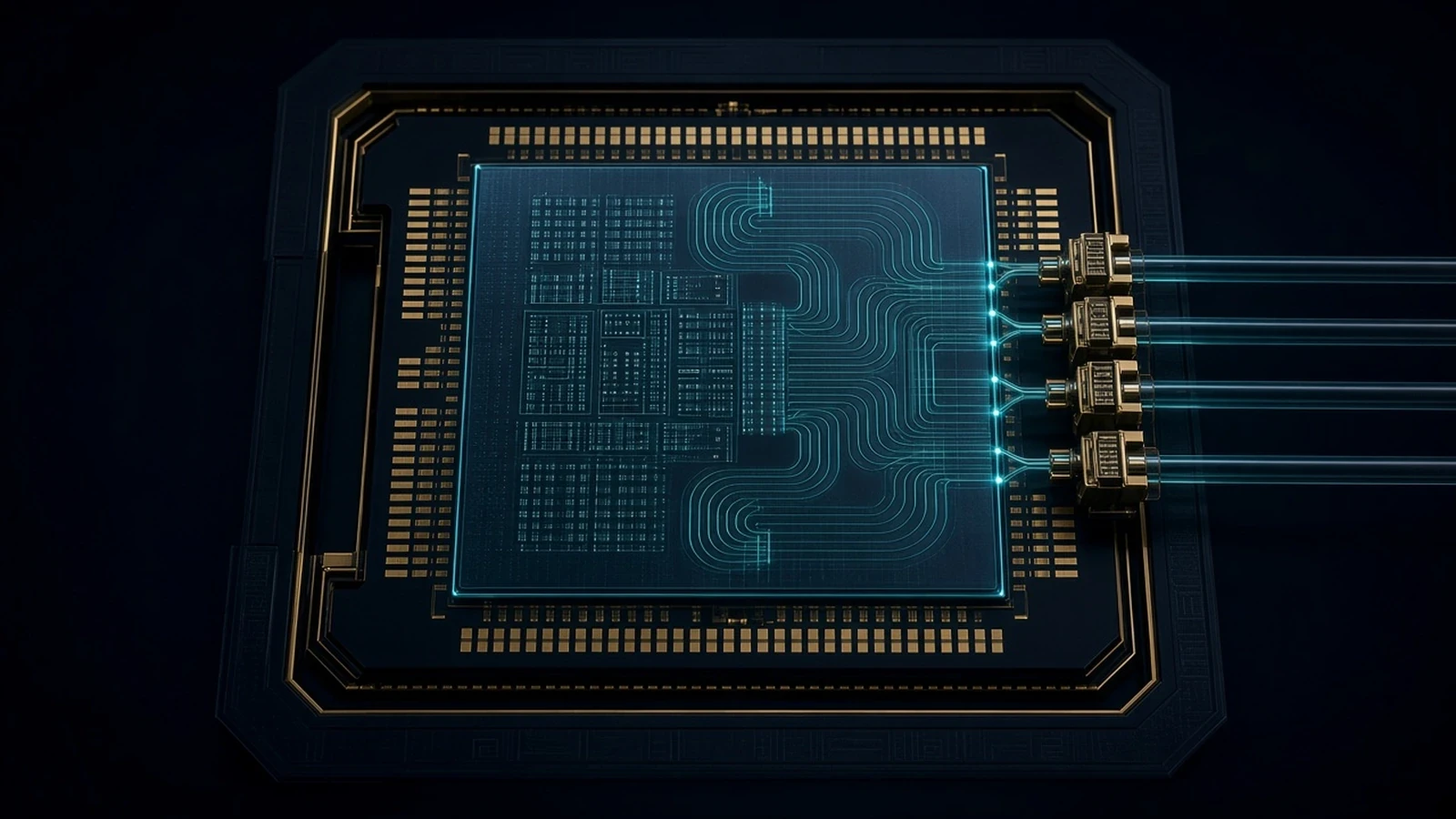
Intel silicon photonics platform combining photonic integrated circuits and on-chip lasers for optical connectivity products. Optical compute interconnect remains part of this platform, not a separate listing.
Data CenterTelecommunicationsView Technology
KLA wafer defect inspection and review systems used to find, classify and monitor particles and pattern defects. Distinct from overlay and dimensional metrology.
AutomotiveData CenterConsumer ElectronicsView Technology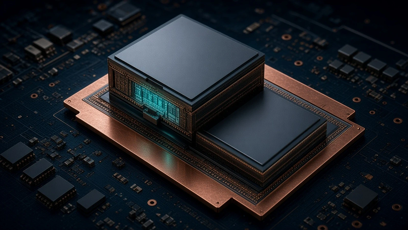
Cadence design platform for planning, implementing and analyzing 2.5D and 3D multi-die / chiplet systems.
AutomotiveAI & HPCData CenterView Technology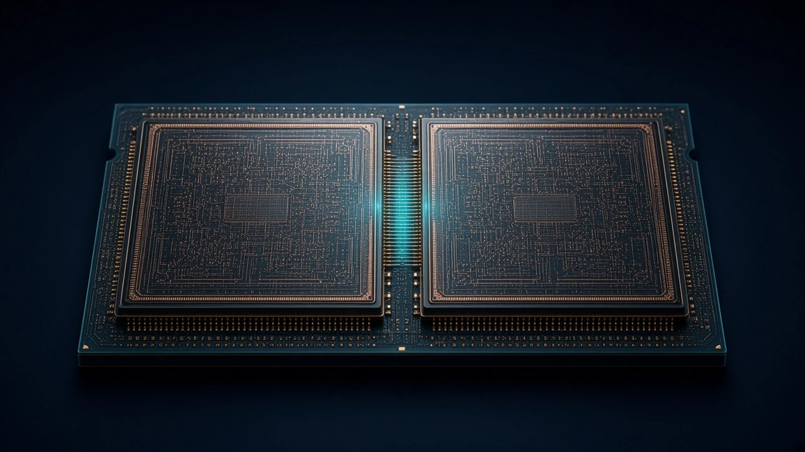
Synopsys die-to-die IP solution for Universal Chiplet Interconnect Express, including controller, PHY and verification IP.
AutomotiveAI & HPCData CenterView Technology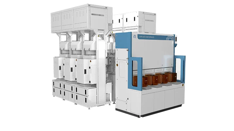
Modular semiconductor wafer-manufacturing chassis from Applied Materials for combining multiple chamber types on one system. Distinct from the Endura metallization platform.
AI & HPCData CenterView Technology
Lam Research wafer-process equipment category for thin-film deposition, plasma etch, strip, clean and related fabrication steps. SABRE ECD is listed separately.
Data CenterConsumer ElectronicsView Technology
Intel Foundry 3D stacking and 2.5D chiplet packaging family, including hybrid-bonding options described as Foveros Direct 3D. EMIB is a separate 2.5D bridge platform.
AI & HPCData CenterConsumer ElectronicsView Technology