VERTICALLY STACKED NAND
Vertically stacked NAND flash technology family
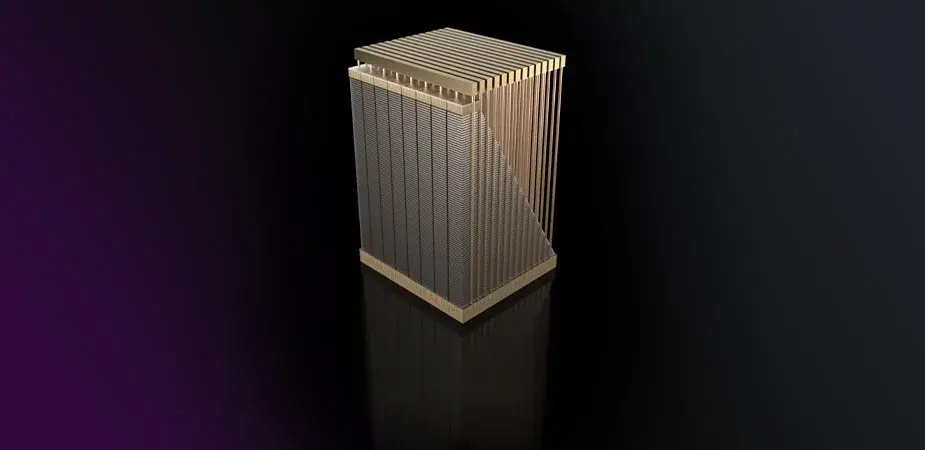
Vertically stacked NAND flash technology family
Described for data-center, client, mobile and automotive storage designs
Automotive · AI & HPC · Data Center · +1
Public source
Micron 3D NAND is a publicly described vertically stacked NAND flash technology used as the semiconductor storage building block beneath finished storage products.
Official technology image
Micron 3D NAND is a vertically stacked NAND flash technology family used as the semiconductor storage building block in data-center, client, mobile and automotive designs.
Official Micron NAND pages describe successive process generations, including ninth-generation (G9) 3D TLC NAND, as evolution of this family rather than independent technologies. Solid-state drive models, UFS products and specific capacities are implementations of this NAND technology, not separate listings. This independent listing identifies the 3D NAND technology family, not consumer storage products. Interface rates and generation details should be taken from Micron's current NAND documentation.
Key characteristics associated with this technology.
Vertically stacked NAND flash technology family
G9 and other process generations remain family evolution, not separate listings
Described for data-center, client, mobile and automotive storage designs
SSD models, UFS products and capacities are implementations, not separate listings
Explore other semiconductor technologies.
Ultra-low-power connected-device system-on-chip that Sensesemi describes with wireless connectivity, a microcontroller, and an edge AI accelerator.
Consumer ElectronicsMedicalView Technology
Aheesa's Vihaan-I is a RISC-V networking SoC for fiber broadband. First-pass silicon was announced in 2026, with production tape-out targeted for 2027.
AutomotiveIndustrialView Technology
Kulicke & Soffa APTURA is a thermo-compression bonder for advanced packaging, not a wire bonder catalog and not OSAT assembly.
AI & HPCData CenterView Technology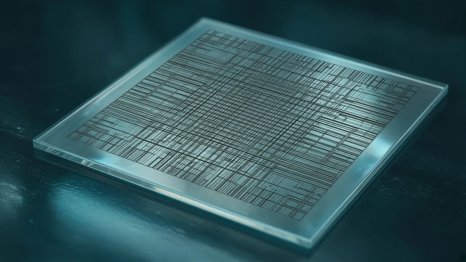
Photronics advanced IC photomasks are lithography reticles for integrated circuits, not a foundry node and not FPD masks.
AutomotiveAI & HPCView Technology