Discover 169 technologies from leading innovators around the world.
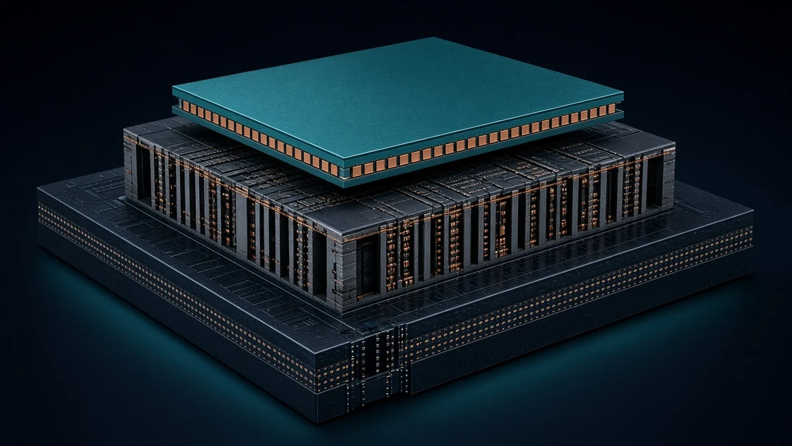
3D V-Cache stacks an L3 cache tile on a CPU core-complex die using copper-to-copper hybrid bonding and TSVs. Official AMD materials call it the first x86 true 3D die stack, with much higher interconnect density versus 2D chiplets.
AI & HPCData CenterConsumer ElectronicsView Technology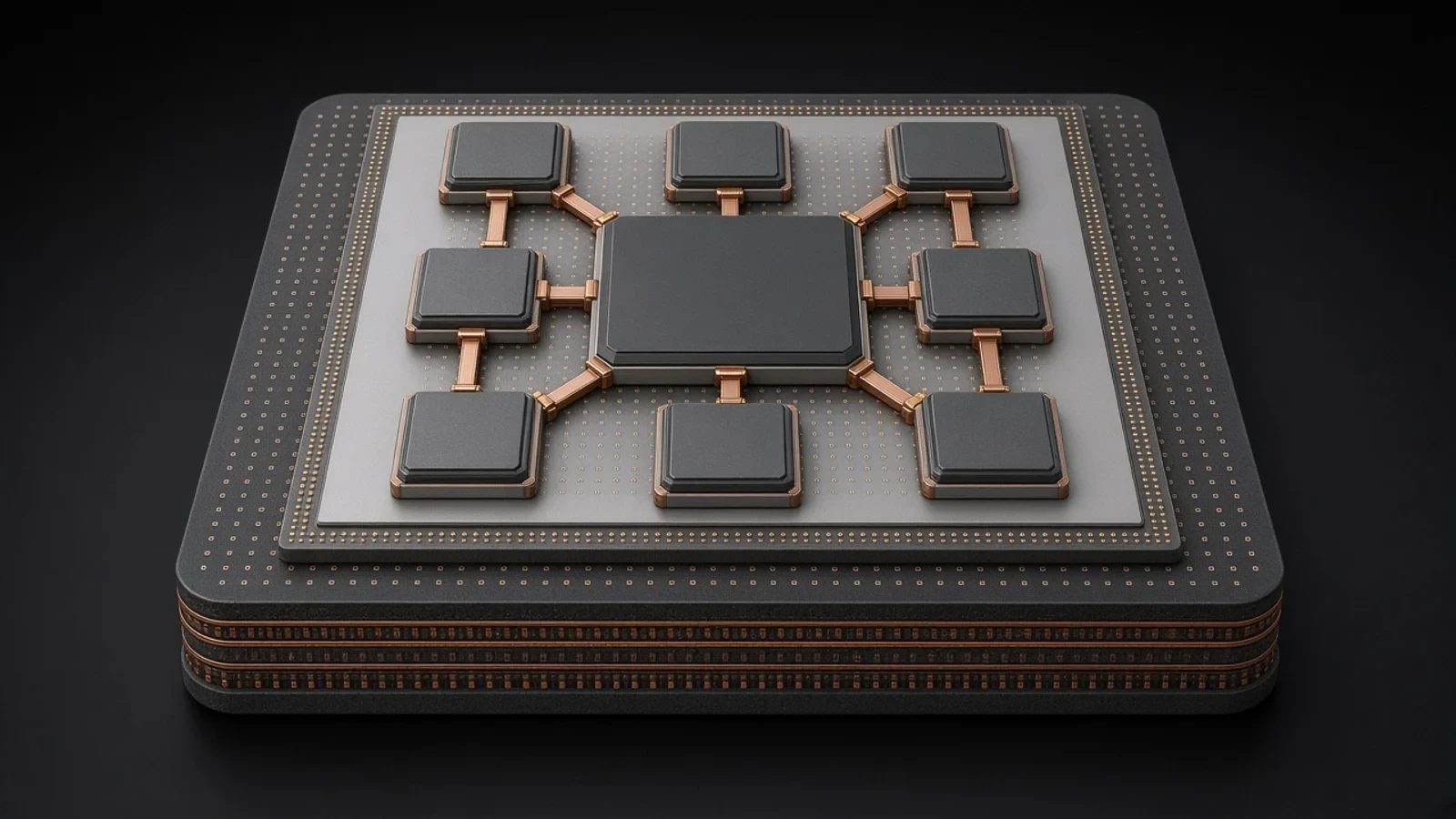
Infinity Fabric is AMD’s coherent on-package and multi-die interconnect, linking CPU core-complex dies to a central I/O die and, in multi-socket systems, across packages. Official EPYC architecture documents describe CCD–IOD GMI links and xGMI.
AI & HPCData CenterConsumer Electronics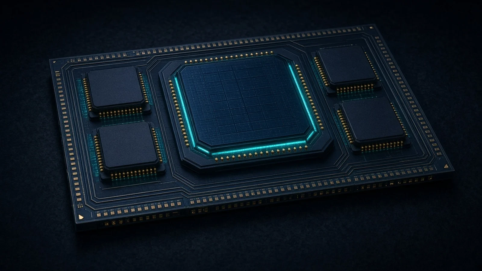
Apple Silicon is Apple’s fabless SoC platform. The M1 newsroom introduction defines a system-on-chip with CPU, GPU, Neural Engine, I/O and unified memory on a single package so those engines share one memory pool.
AI & HPCConsumer ElectronicsView Technology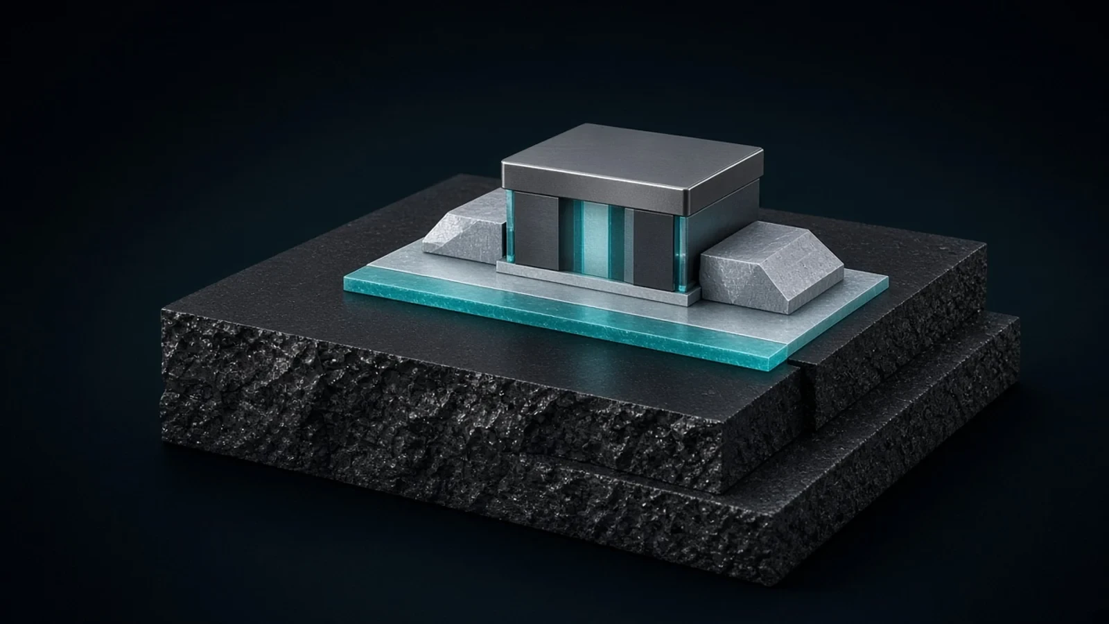
22FDX is GlobalFoundries’ 22 nm fully depleted SOI platform: a thin-body transistor on an insulating layer, targeting low-power, RF, automotive and IoT designs that do not need leading-edge GAA.
AutomotiveConsumer ElectronicsTelecommunications+1
Filogic is MediaTek’s Wi-Fi 6/6E/7 connectivity platform for routers, gateways, access points and clients, with Multi-Link Operation, 320 MHz channels, 4096-QAM and dedicated NPUs on flagship access-point chips.
Consumer ElectronicsTelecommunicationsIoTView Technology
FastConnect 7900 is a 6 nm single-chip connectivity system integrating Wi-Fi 7, Bluetooth and UWB, with High Band Simultaneous Multi-Link and companion RF front-end modules.
Consumer ElectronicsTelecommunicationsIoTView Technology
Oryon is Qualcomm’s custom 64-bit CPU microarchitecture, including cache hierarchy, branch prediction, prefetch and later Flex Cache, designed in-house and scaled across Snapdragon platforms.
AutomotiveAI & HPCData Center+1View Technology
Samsung’s 3 nm foundry node introduced Gate-All-Around transistors as Multi-Bridge-Channel FETs (MBCFET): stacked nanosheet channels with the gate on all four sides, replacing FinFET for better electrostatic control.
AutomotiveAI & HPCData Center+1View Technology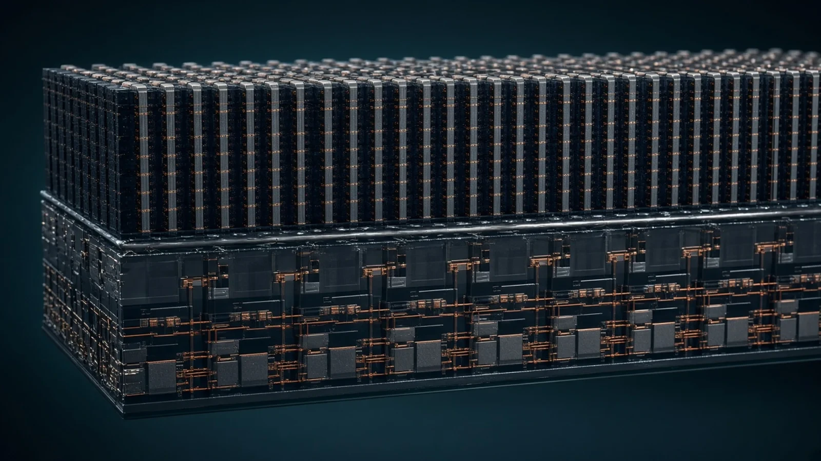
Samsung V10 BV-NAND is bonded vertical NAND with more than 400 word lines, brought to mass-production readiness for AI storage.
AI & HPCData CenterConsumer ElectronicsView Technology
Snapdragon X80 is Qualcomm's 5G Modem-RF system, combining the modem and RF front end, with 5G Advanced features and NB-NTN satellite support.
AutomotiveConsumer ElectronicsTelecommunicationsView Technology
Sony’s stacked CMOS image sensor separates the pixel die from the logic die and joins them with Cu-Cu hybrid bonding, replacing TSVs. Official technology pages describe Cu-Cu as enabling denser, smaller, higher-function sensors.
AutomotiveIndustrialConsumer Electronics+1
Micron 3D NAND is a vertically stacked NAND flash technology family used as the semiconductor storage building block in data-center, client, mobile and automotive designs.
AutomotiveAI & HPCData Center+1View Technology
Micron LPDDR is a low-power DRAM family for mobile, client, automotive and data-center designs that need high bandwidth at reduced power. LPDDR generations remain one technology line.
AutomotiveAI & HPCData Center+1View Technology
Micron GDDR is a discrete graphics DRAM family spanning GDDR6, GDDR6X and GDDR7 generations for GPUs, gaming systems and AI inference accelerators.
AI & HPCConsumer ElectronicsView Technology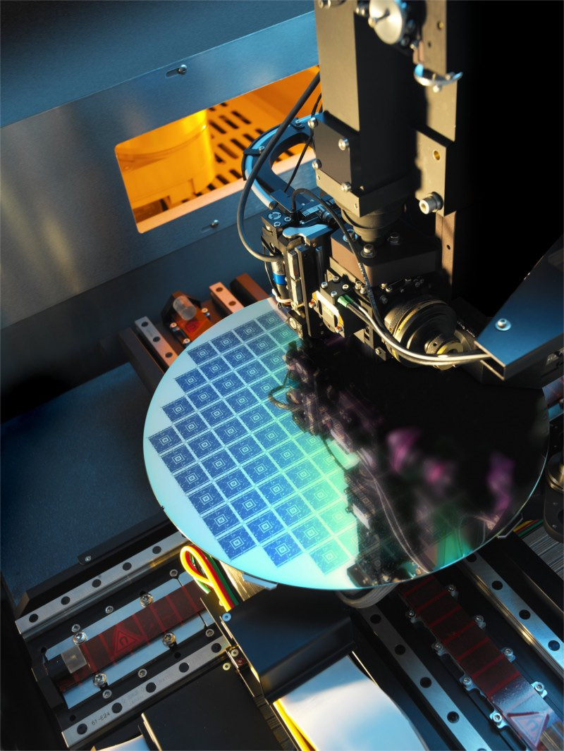
KLA overlay and dimensional metrology systems measure layer-to-layer alignment, critical dimensions and related pattern geometry. Distinct from defect inspection and review.
AutomotiveData CenterConsumer ElectronicsView Technology
ASML TWINSCAN DUV is the deep-ultraviolet lithography platform covering immersion and dry scanners that print most chip layers alongside EUV. Distinct from NXE and High-NA EXE EUV.
AI & HPCConsumer ElectronicsView Technology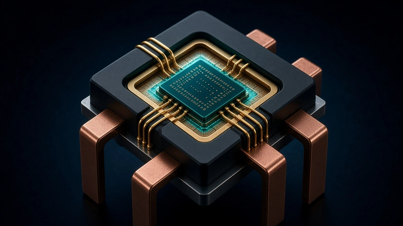
Infineon CoolMOS is a high-voltage silicon superjunction MOSFET technology family for offline and high-voltage power conversion, distinct from CoolSiC, CoolGaN and OptiMOS.
Data CenterIndustrialConsumer Electronics+1View Technology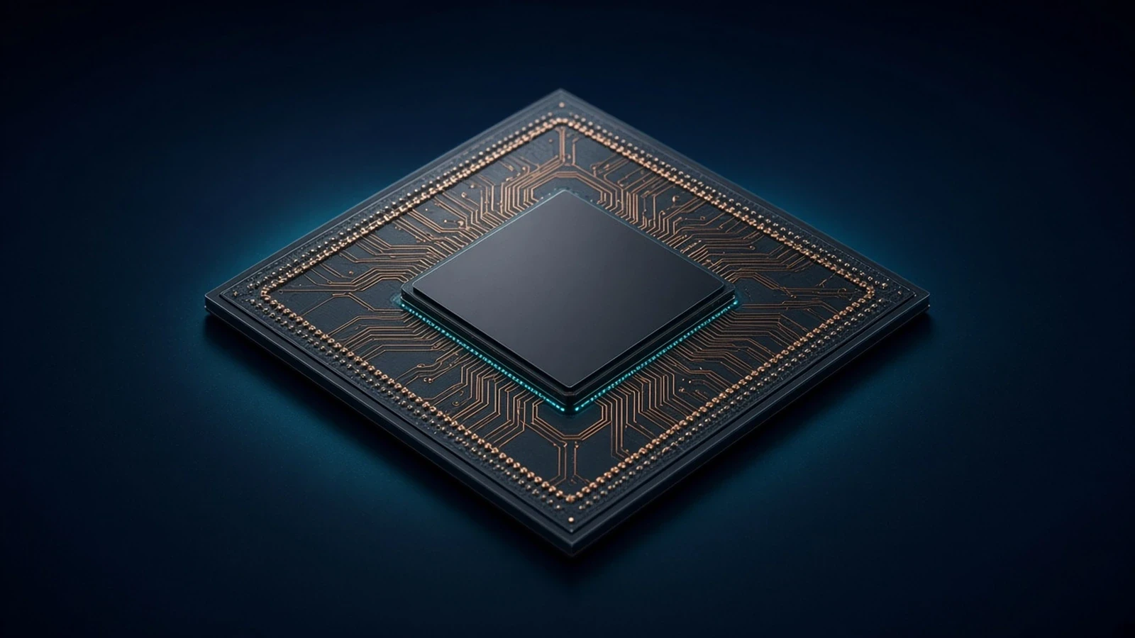
TSMC InFO is a wafer-level integrated fan-out packaging platform using high-density redistribution layers for mobile, network and high-performance computing integration.
AI & HPCConsumer ElectronicsTelecommunicationsView Technology
ASML TWINSCAN NXE is the 0.33 numerical-aperture EUV lithography platform used in high-volume manufacturing of advanced logic and memory chips. Distinct from High-NA EXE systems.
AI & HPCConsumer ElectronicsView Technology
Mindgrove Secure IoT is a RISC-V-based microcontroller/SoC family for connected and embedded devices, combining a processor core with peripherals, hardware crypto accelerators and on-chip secure memory.
IndustrialConsumer ElectronicsIoTView Technology
Pragmatic FlexIC Platform Gen 3 is a flexible semiconductor technology platform using metal-oxide thin-film transistors on flexible substrates for mixed-signal integrated circuits supporting connect, sense and basic compute functions.
IndustrialConsumer ElectronicsIoTView Technology
ASM Atomic Layer Deposition technology enables highly controlled, layer-by-layer deposition of ultrathin conformal films for advanced semiconductor logic, memory and packaging structures.
AI & HPCData CenterConsumer ElectronicsView Technology
Bosch MEMS sensor technology uses microelectromechanical structures to translate physical changes such as motion, pressure and environmental conditions into electrical information for compact sensing applications.
IndustrialConsumer ElectronicsIoTView Technology
KLA wafer defect inspection and review systems used to find, classify and monitor particles and pattern defects. Distinct from overlay and dimensional metrology.
AutomotiveData CenterConsumer ElectronicsView Technology