Discover 169 technologies from leading innovators around the world.
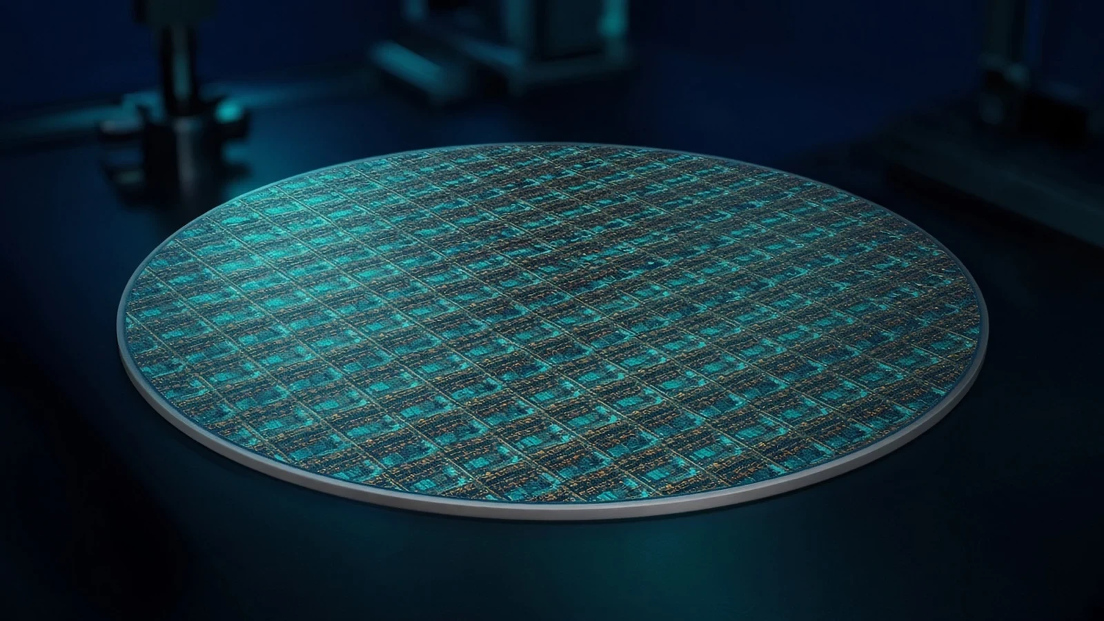
Cerebras Wafer-Scale Engine 3 is a wafer-scale AI processor: one chip occupying an entire 300mm wafer for large-model training and inference.
AI & HPCData CenterView Technology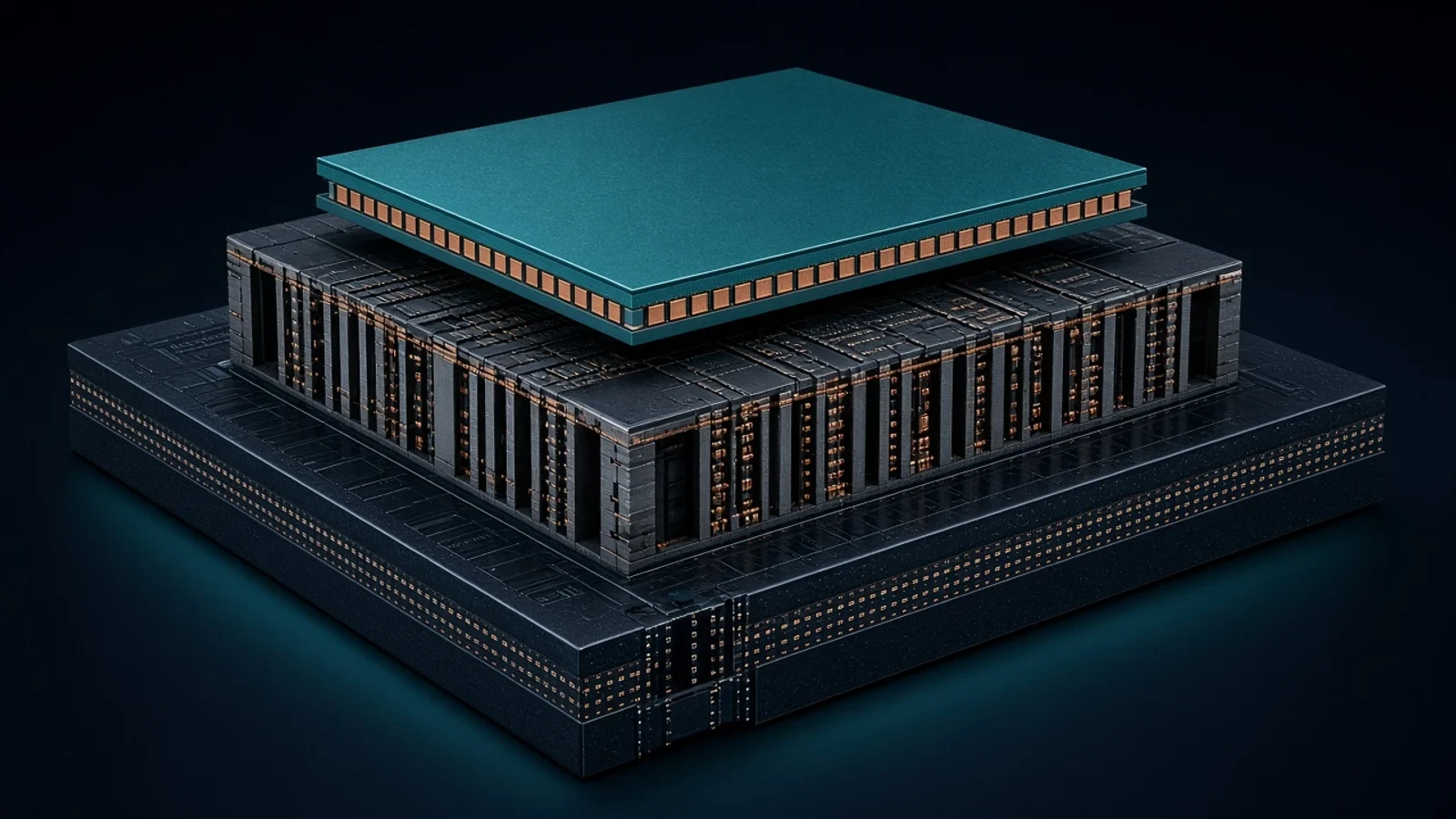
3D V-Cache stacks an L3 cache tile on a CPU core-complex die using copper-to-copper hybrid bonding and TSVs. Official AMD materials call it the first x86 true 3D die stack, with much higher interconnect density versus 2D chiplets.
AI & HPCData CenterConsumer ElectronicsView Technology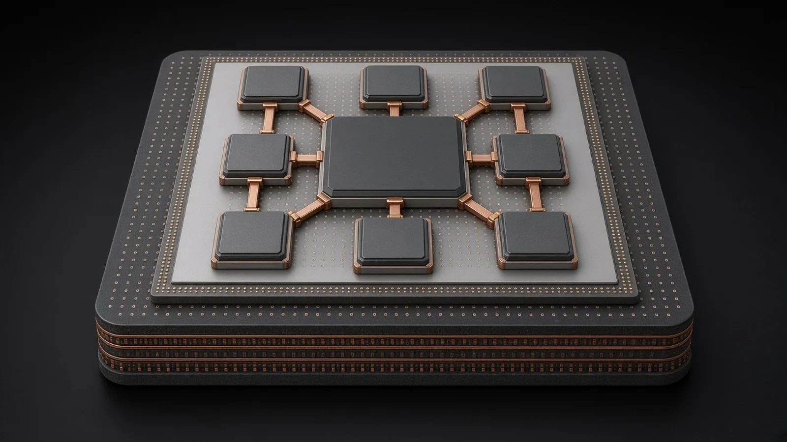
Infinity Fabric is AMD’s coherent on-package and multi-die interconnect, linking CPU core-complex dies to a central I/O die and, in multi-socket systems, across packages. Official EPYC architecture documents describe CCD–IOD GMI links and xGMI.
AI & HPCData CenterConsumer ElectronicsView Technology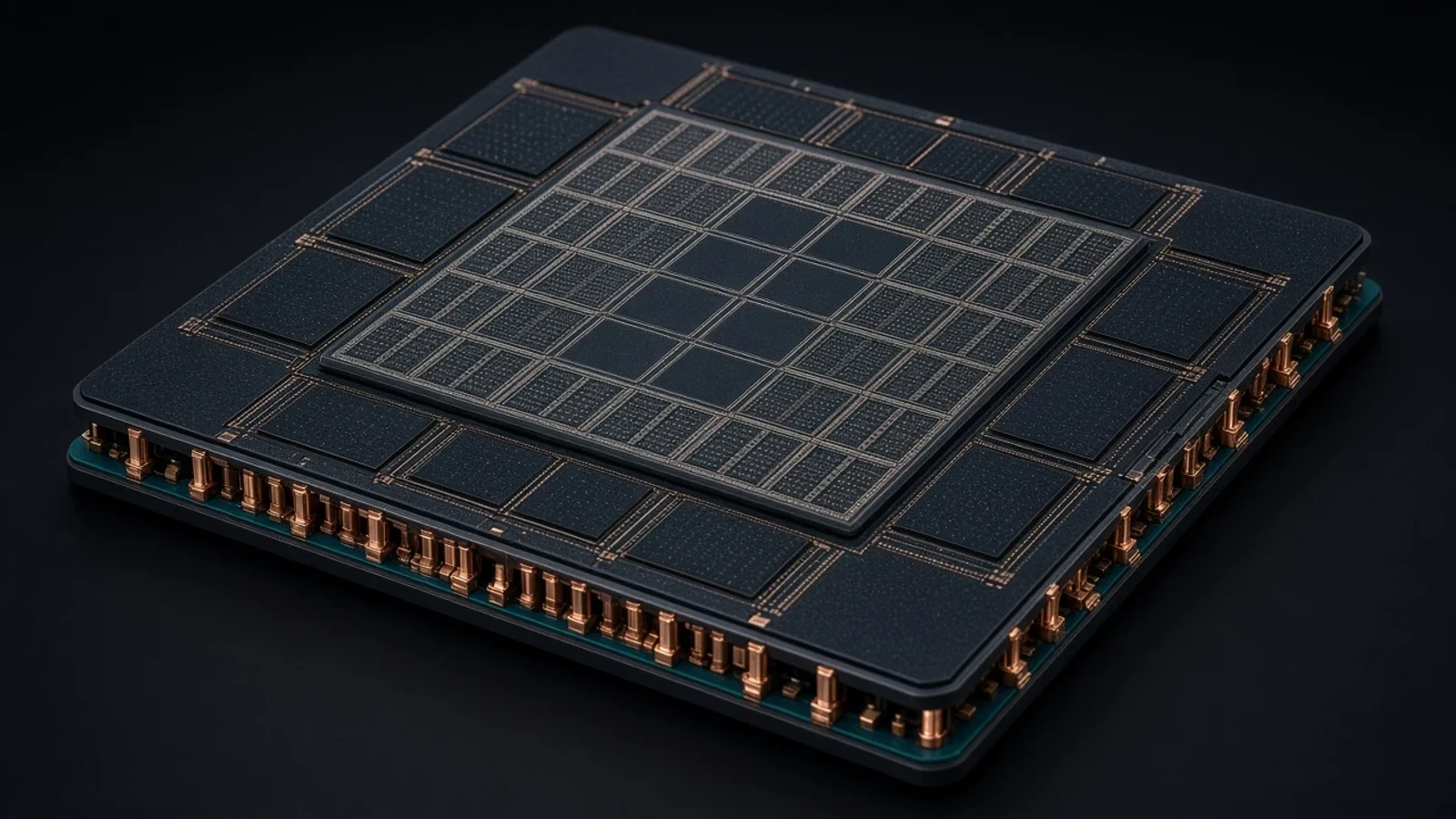
Trainium is AWS’s custom machine-learning training silicon, built around NeuronCore and used in EC2 Trn instances. Official AWS silicon pages describe purpose-built ML chips as part of AWS custom silicon.
AI & HPCData CenterView Technology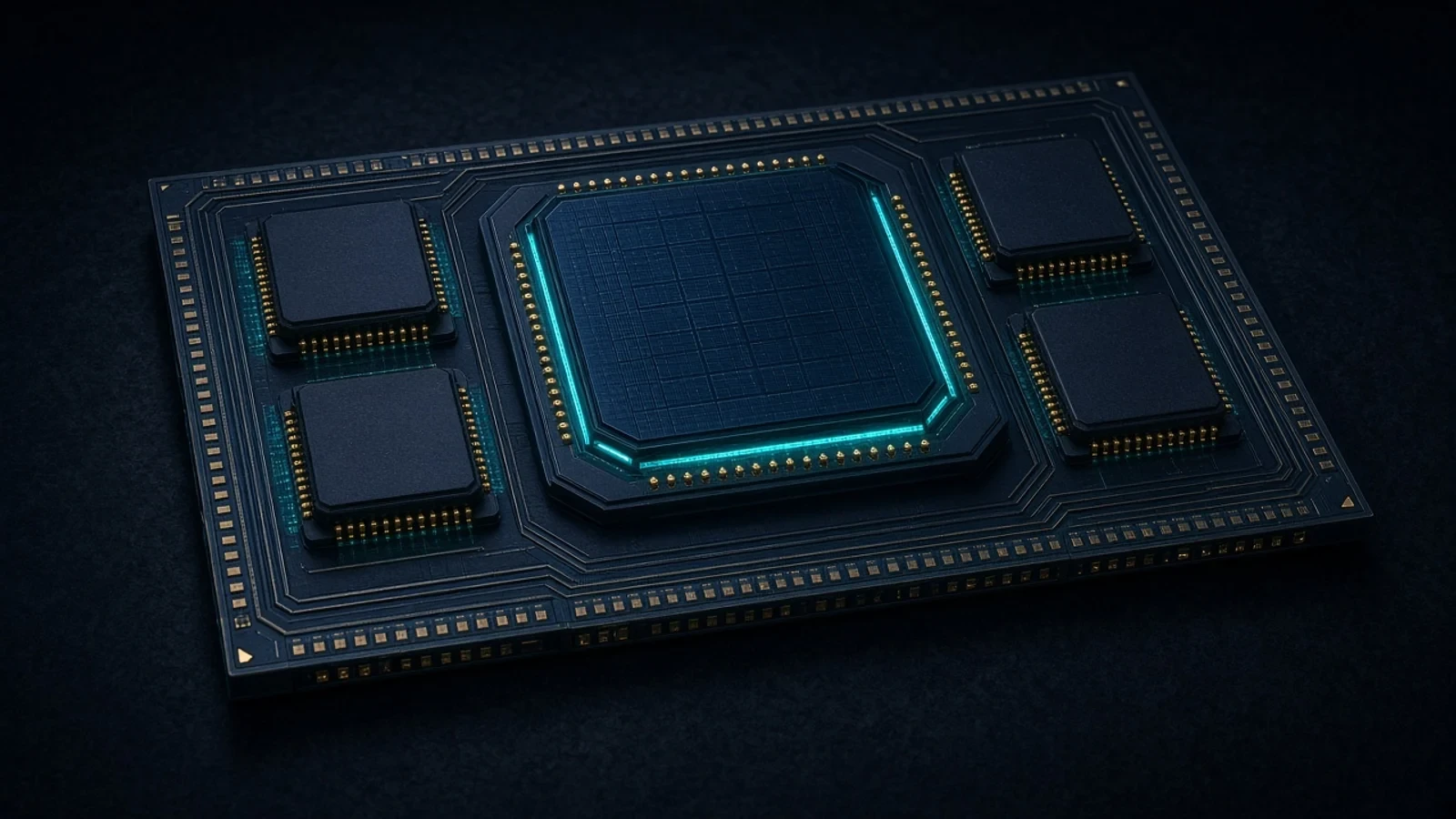
Apple Silicon is Apple’s fabless SoC platform. The M1 newsroom introduction defines a system-on-chip with CPU, GPU, Neural Engine, I/O and unified memory on a single package so those engines share one memory pool.
AI & HPCConsumer ElectronicsView Technology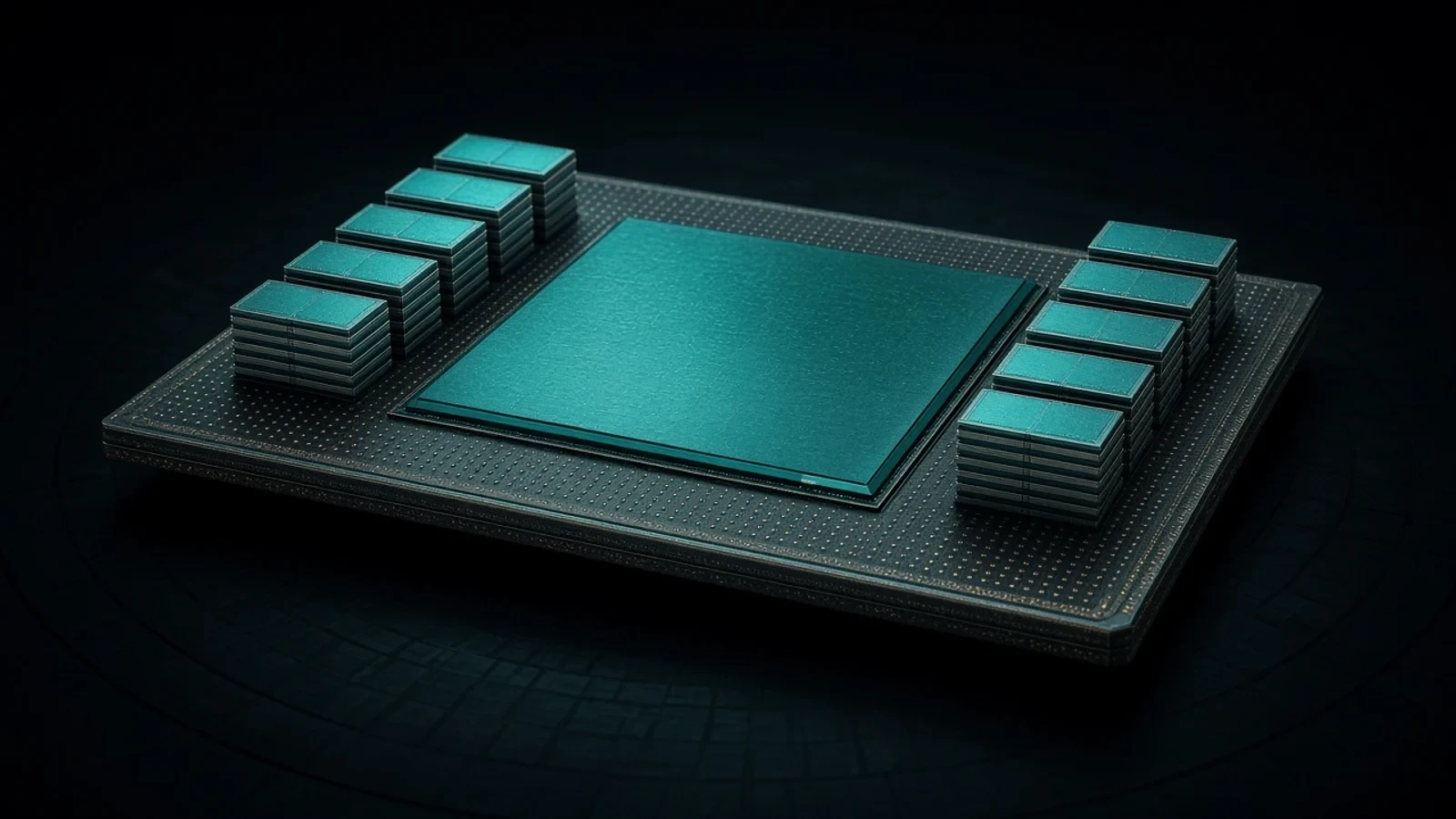
Azure Maia 100 is Microsoft's first in-house cloud AI accelerator: 105 billion transistors on 5 nm, for Azure training and inference.
AI & HPCData CenterView Technology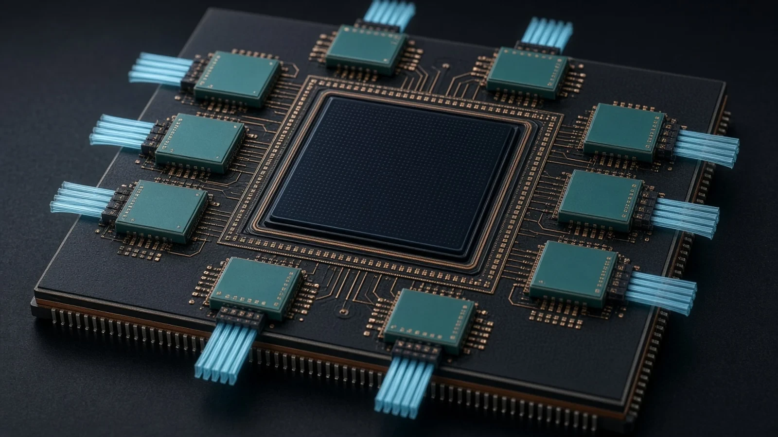
Broadcom’s CPO platform heterogeneously integrates optical engines (TSMC COUPE) with Ethernet switch silicon. Tomahawk 6–Davisson is the third-generation CPO switch: 102.4 Tbps optically enabled capacity and a claimed reduction in optical-interconnect power versus pluggables.
AI & HPCData CenterTelecommunicationsView Technology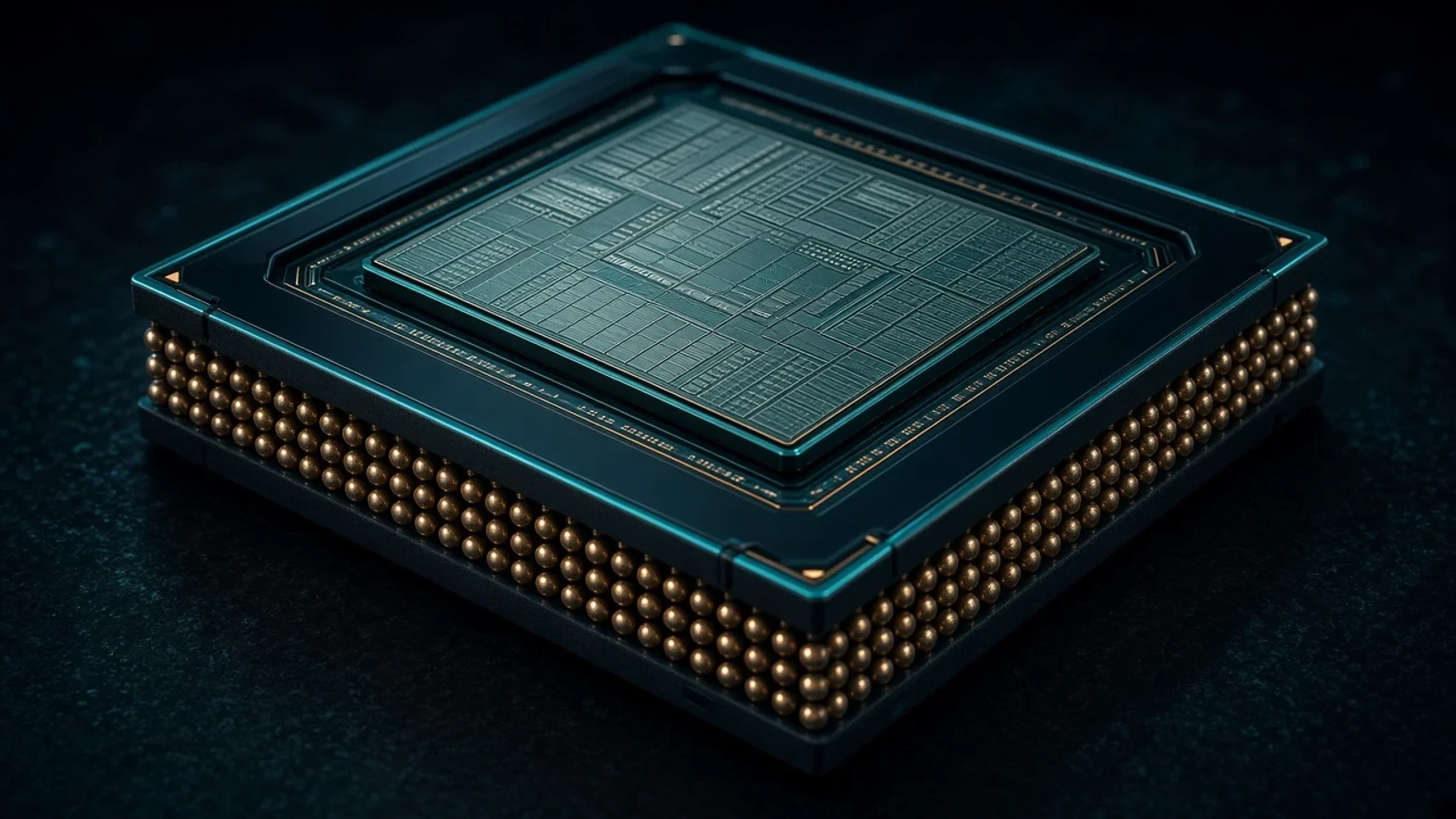
Tomahawk is Broadcom’s Ethernet switch-ASIC family for data-center and AI fabrics. Tomahawk 6 is the current generation: 102.4 Tbps in a single chip, 100G/200G SerDes, and an optional co-packaged optics variant.
AI & HPCData CenterTelecommunications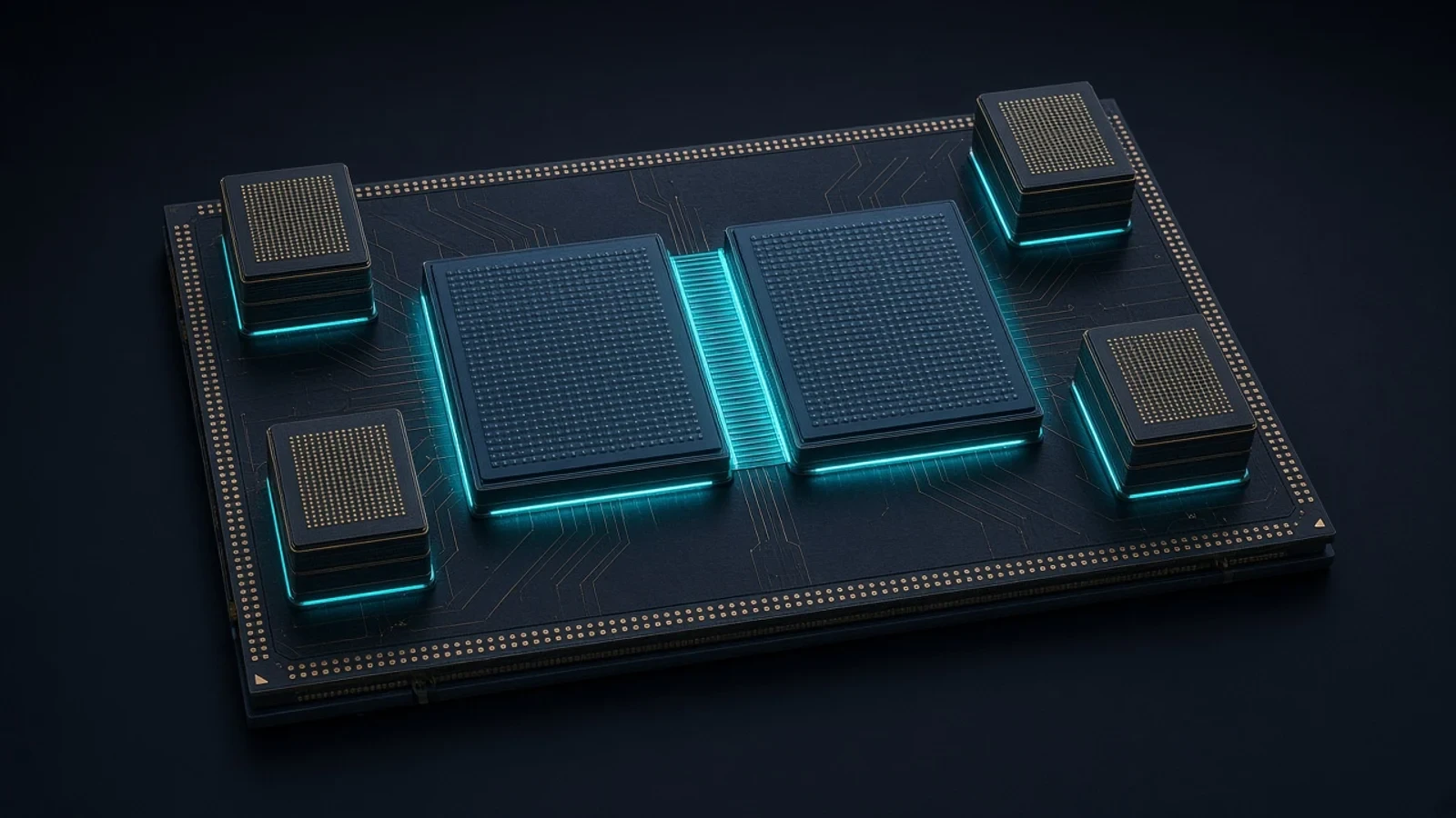
Blackwell is NVIDIA’s current data-center GPU architecture, built as a dual-die GPU with a 10 TB/s chip-to-chip interconnect. Official materials describe a two-reticle design manufactured on TSMC 4NP.
AI & HPCData CenterView Technology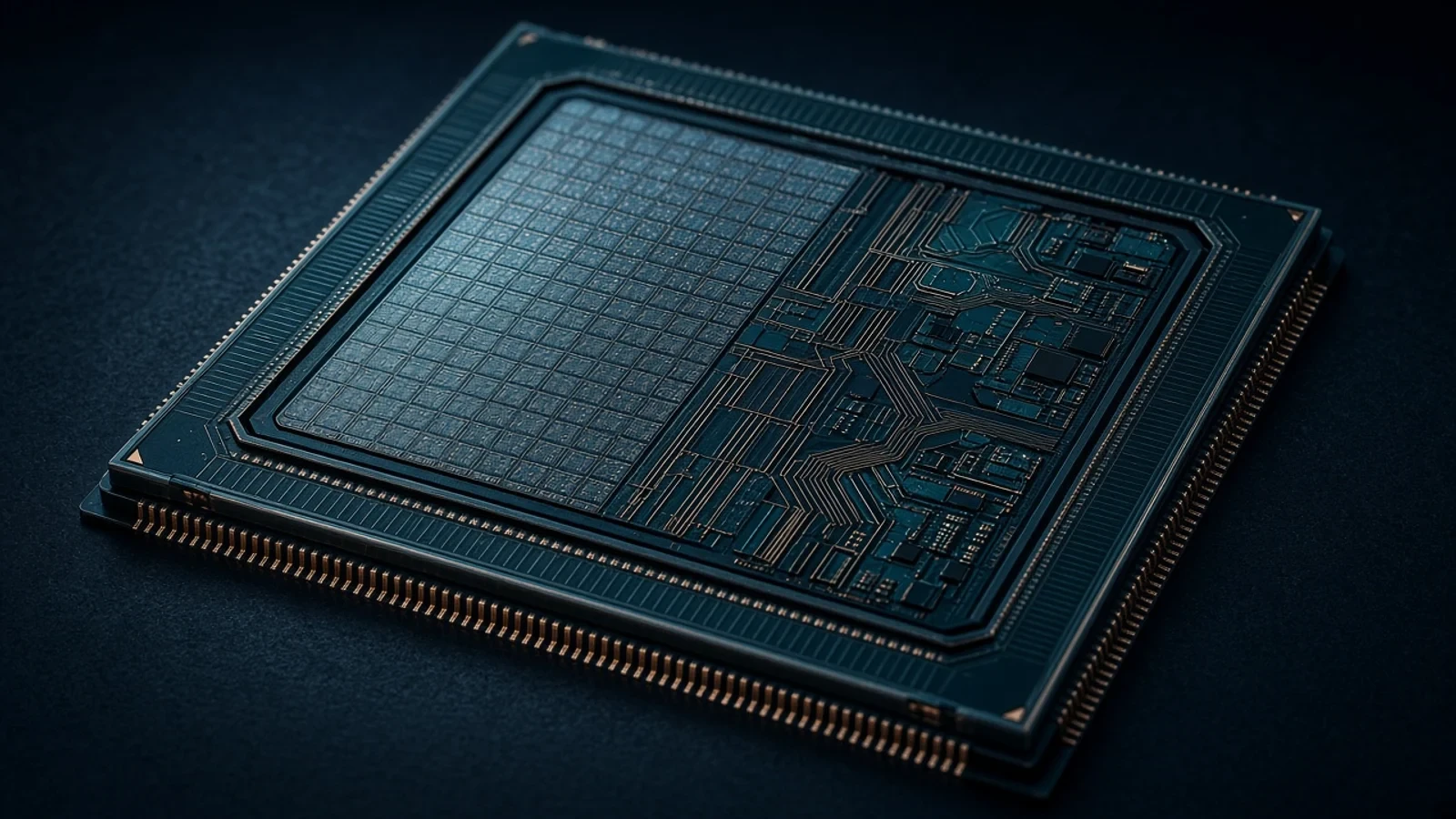
BlueField is NVIDIA’s data processing unit: Arm cores, high-speed Ethernet/InfiniBand and hardware accelerators for networking, storage and security offload, isolated from the host CPU.
AI & HPCData CenterTelecommunicationsView Technology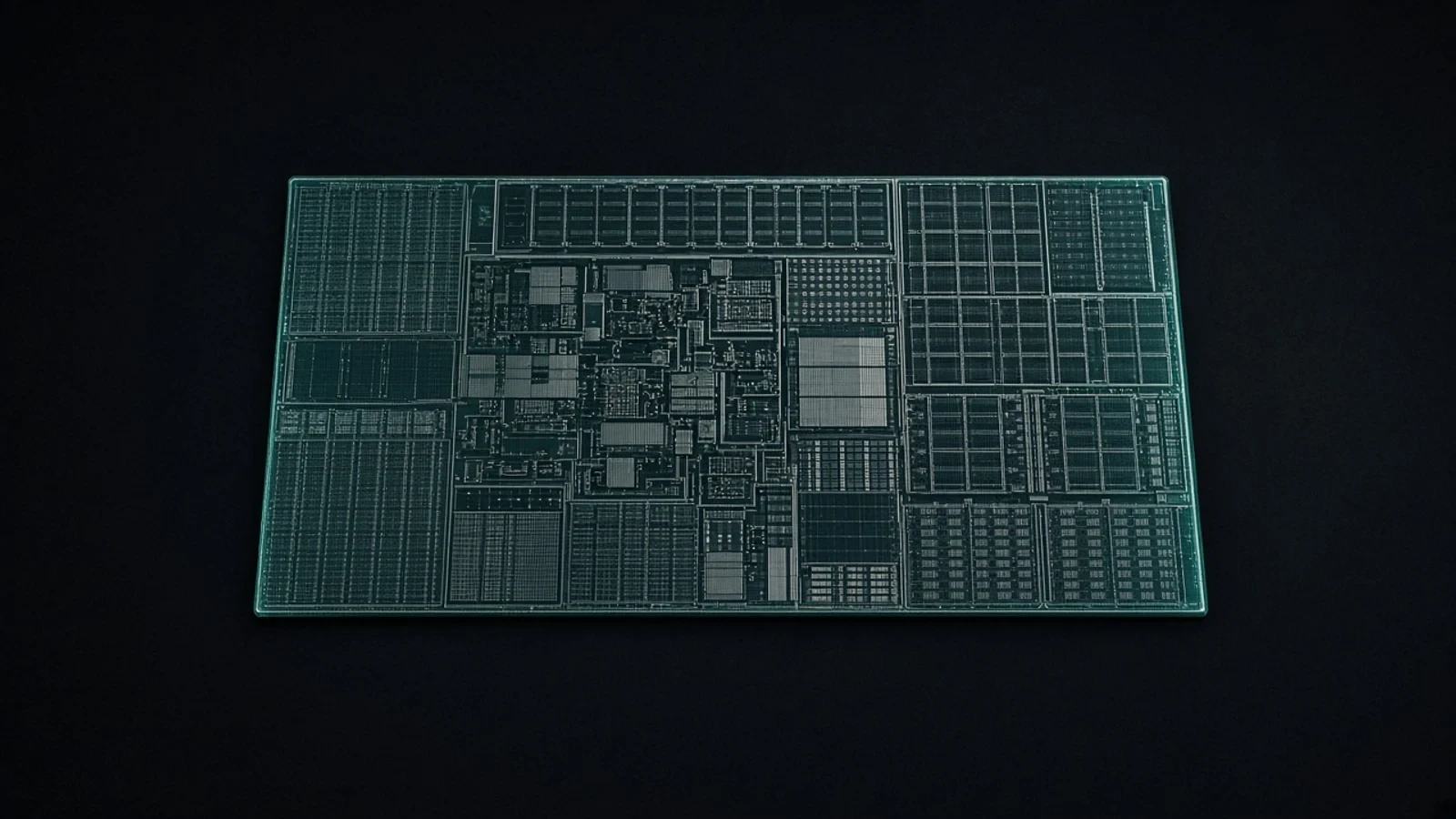
Oryon is Qualcomm’s custom 64-bit CPU microarchitecture, including cache hierarchy, branch prediction, prefetch and later Flex Cache, designed in-house and scaled across Snapdragon platforms.
AutomotiveAI & HPCData Center+1View Technology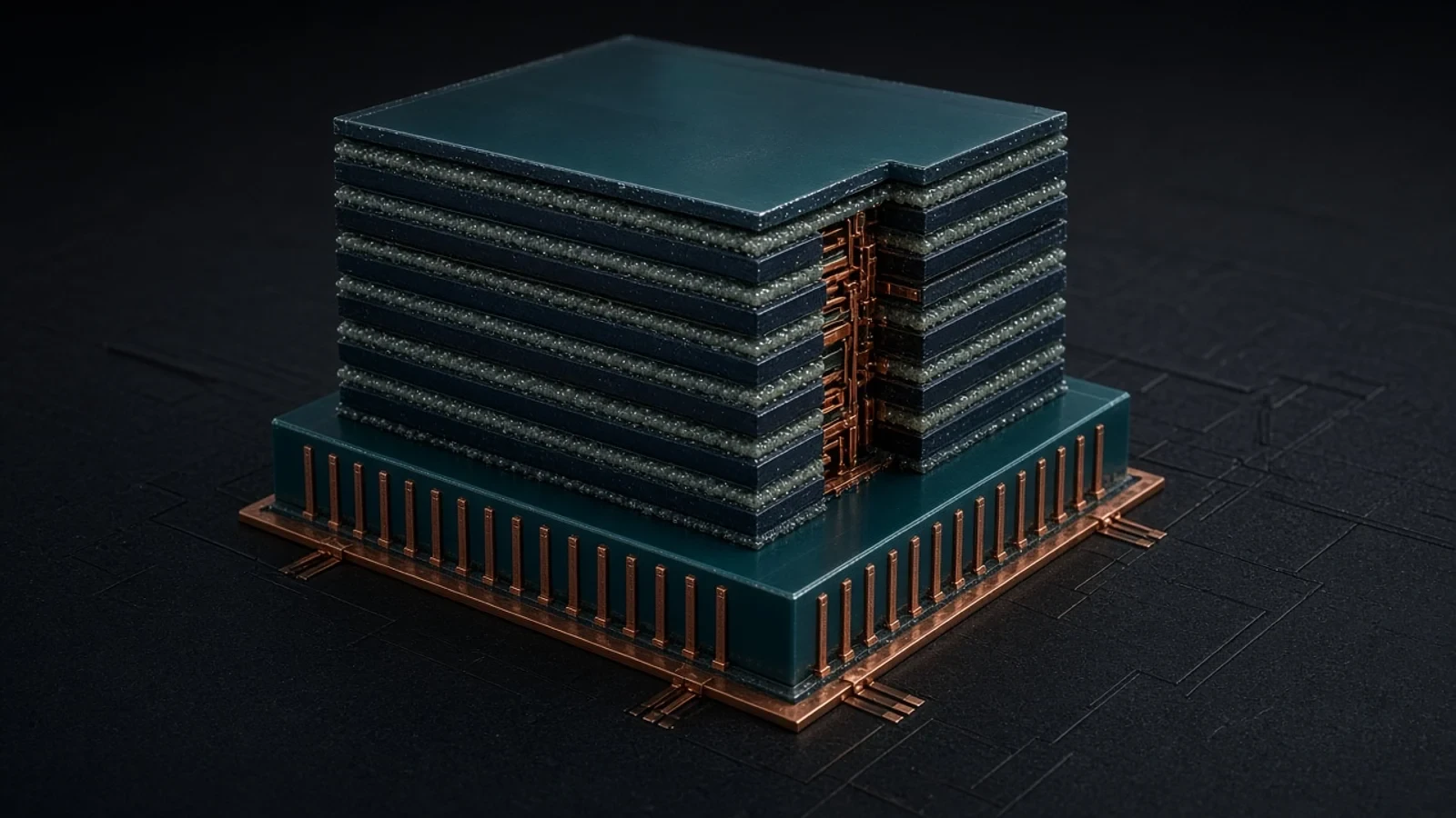
SK hynix HBM4 doubles I/O to 2,048 terminals, claims >10 Gbps and more than 40% better power efficiency versus the prior generation, and uses Advanced MR-MUF to stack DRAM with warpage control and heat dissipation.
AI & HPCData CenterView Technology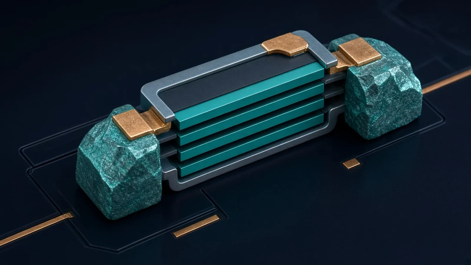
Samsung’s 3 nm foundry node introduced Gate-All-Around transistors as Multi-Bridge-Channel FETs (MBCFET): stacked nanosheet channels with the gate on all four sides, replacing FinFET for better electrostatic control.
AutomotiveAI & HPCData Center+1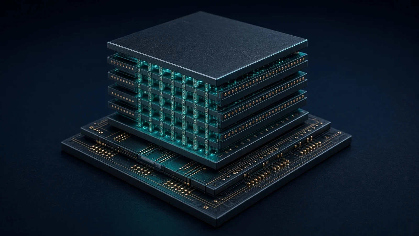
Samsung HBM4 is the company’s current high-bandwidth DRAM stack for AI accelerators, with an advanced base die and stacked DRAM cubes. Samsung’s official HBM family page covers HBM3E through HBM4/HBM4E as the AI-memory roadmap.
AI & HPCData CenterView Technology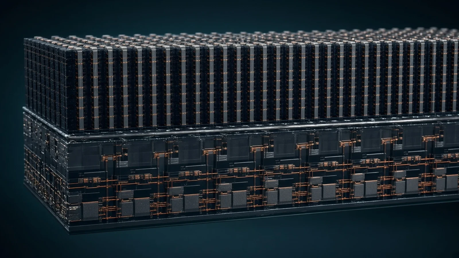
Samsung V10 BV-NAND is bonded vertical NAND with more than 400 word lines, brought to mass-production readiness for AI storage.
AI & HPCData CenterConsumer ElectronicsView Technology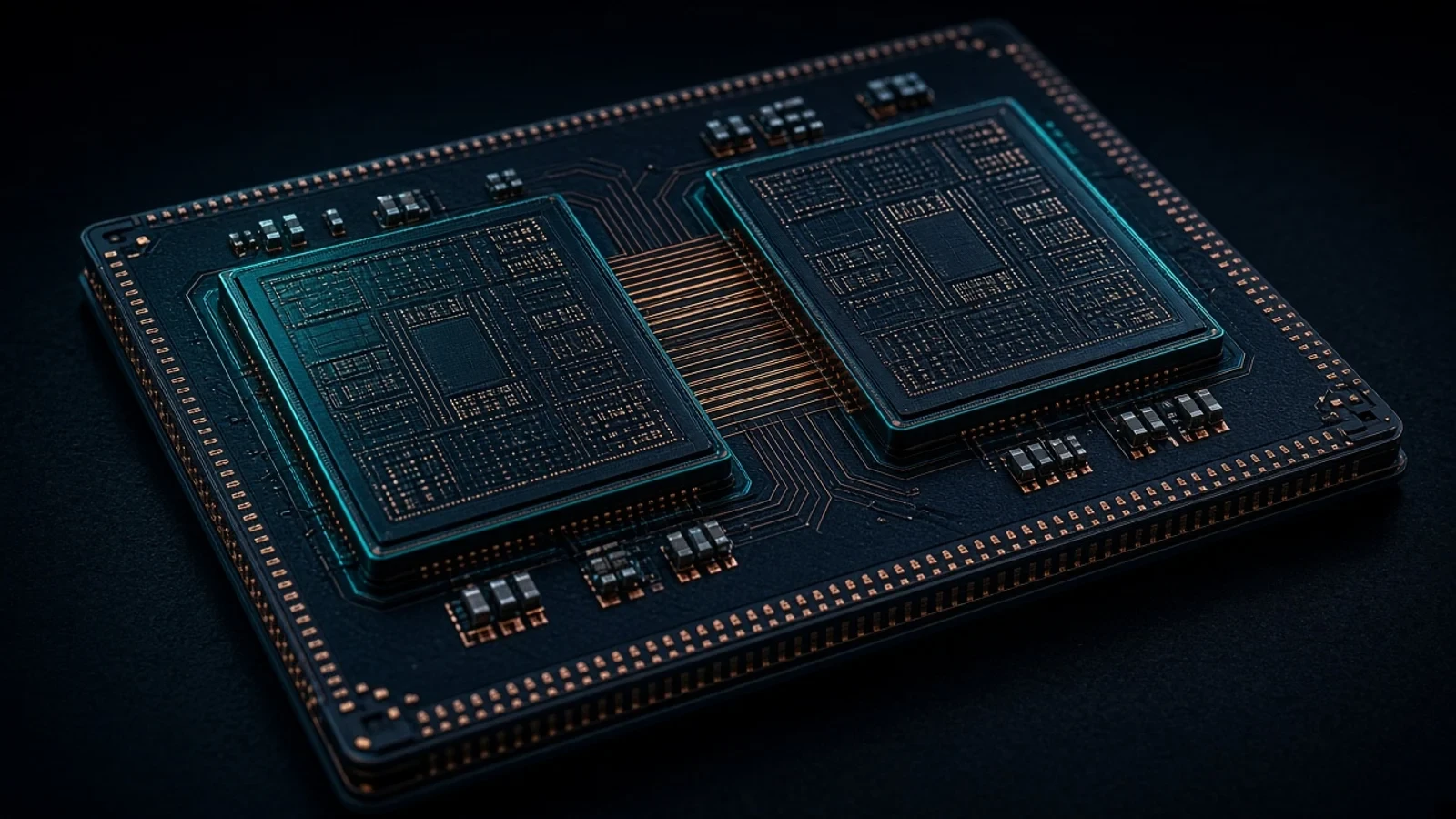
TPU7x (Ironwood) is Google Cloud's seventh-generation TPU, built for large-scale training and inference.
AI & HPCData CenterView Technology
Micron 3D NAND is a vertically stacked NAND flash technology family used as the semiconductor storage building block in data-center, client, mobile and automotive designs.
AutomotiveAI & HPCData Center+1View Technology
Micron LPDDR is a low-power DRAM family for mobile, client, automotive and data-center designs that need high bandwidth at reduced power. LPDDR generations remain one technology line.
AutomotiveAI & HPCData Center+1View Technology
Micron GDDR is a discrete graphics DRAM family spanning GDDR6, GDDR6X and GDDR7 generations for GPUs, gaming systems and AI inference accelerators.
AI & HPCConsumer ElectronicsView Technology
Lam Research SABRE is an electrochemical copper-deposition platform for damascene interconnect, including logic, memory and high-bandwidth memory wiring. Distinct from Lam’s broader etch category.
AI & HPCData CenterView Technology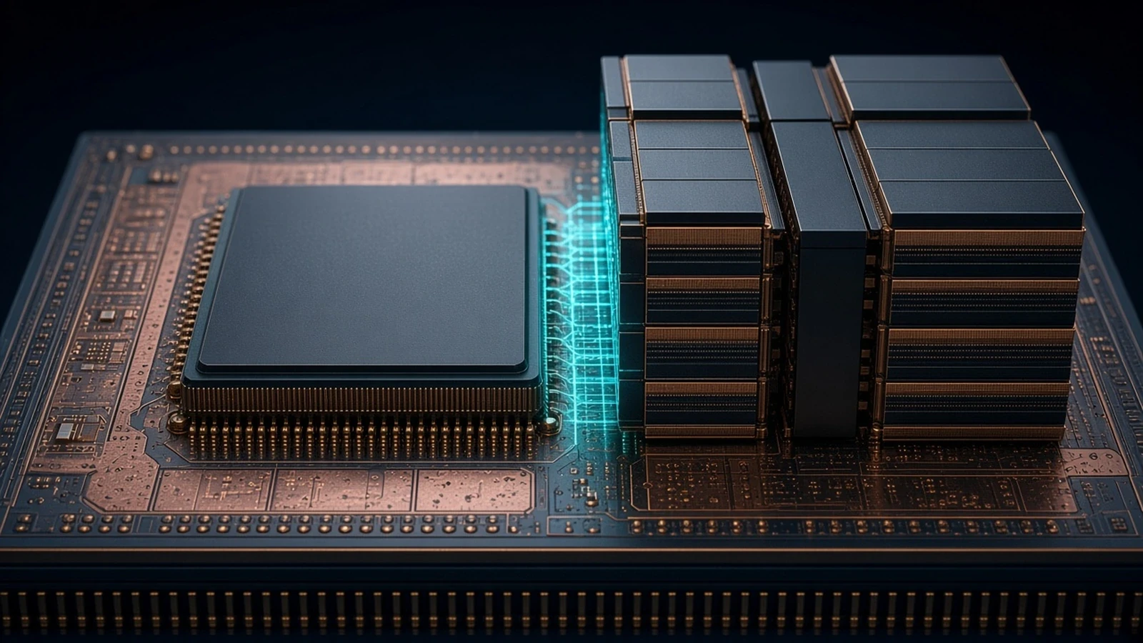
Synopsys HBM interface IP is a high-bandwidth memory interface family including controller, PHY and verification IP for AI and high-performance computing SoCs. Distinct from UCIe die-to-die IP.
AI & HPCData CenterView Technology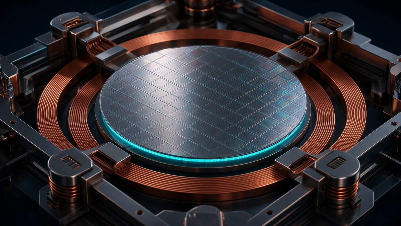
ASM epitaxy is a crystalline film-growth equipment platform covering silicon and silicon-germanium transistor epitaxy and silicon carbide epitaxy. Distinct from ASM atomic layer deposition.
AutomotiveAI & HPCEnergyView Technology
Applied Materials Endura is an ultra-high-vacuum metallization platform used for physical vapor deposition and integrated multi-chamber sequences. Distinct from the Vistara wafer-manufacturing chassis.
AI & HPCData CenterView Technology
ASML TWINSCAN DUV is the deep-ultraviolet lithography platform covering immersion and dry scanners that print most chip layers alongside EUV. Distinct from NXE and High-NA EXE EUV.
AI & HPCConsumer ElectronicsView Technology