Skip to content
Silicon Showcase
CompaniesApplicationsTechnology AreasAbout
Submit Technology
Submit Technology
Silicon Showcase

Silicon Showcase™ is the global directory of semiconductor technologies, platforms and innovations from around the world.

  • Technologies
  • Technology Signals
  • Companies
  • Applications
  • Technology Areas
  • About Us
  • How It Works
  • Submit Technology
  • Contact Us
  • Privacy Policy
  • Terms of Use
  • Disclaimer

Explore

  • Technologies
  • Technology Signals
  • Companies
  • Applications
  • Technology Areas

About

  • About Us
  • How It Works
  • Submit Technology
  • Contact Us

Legal

  • Privacy Policy
  • Terms of Use
  • Disclaimer

© 2026 Silicon Showcase™. All rights reserved.

Explore. Compare. Innovate.

Silicon Showcase
CompaniesApplicationsTechnology AreasAbout
Submit Technology
Submit Technology
Silicon Showcase

Silicon Showcase™ is the global directory of semiconductor technologies, platforms and innovations from around the world.

  • Technologies
  • Technology Signals
  • Companies
  • Applications
  • Technology Areas
  • About Us
  • How It Works
  • Submit Technology
  • Contact Us
  • Privacy Policy
  • Terms of Use
  • Disclaimer

Explore

  • Technologies
  • Technology Signals
  • Companies
  • Applications
  • Technology Areas

About

  • About Us
  • How It Works
  • Submit Technology
  • Contact Us

Legal

  • Privacy Policy
  • Terms of Use
  • Disclaimer

© 2026 Silicon Showcase™. All rights reserved.

Explore. Compare. Innovate.

  1. Home
  2. /Technologies
  3. /Samsung HBM4

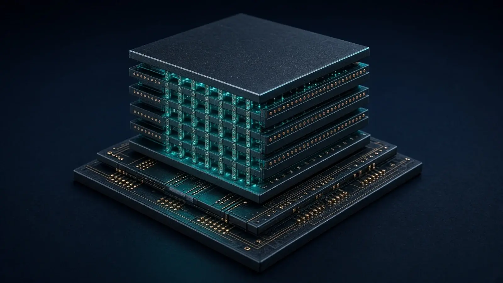
STACKED DRAM CUBES

Stacked DRAM cubes on an advanced HBM base die
CURRENT SAMSUNG AI-MEMORY

Current Samsung AI-memory generation on the official HBM family page

APPLICATIONS

AI & HPC · Data Center

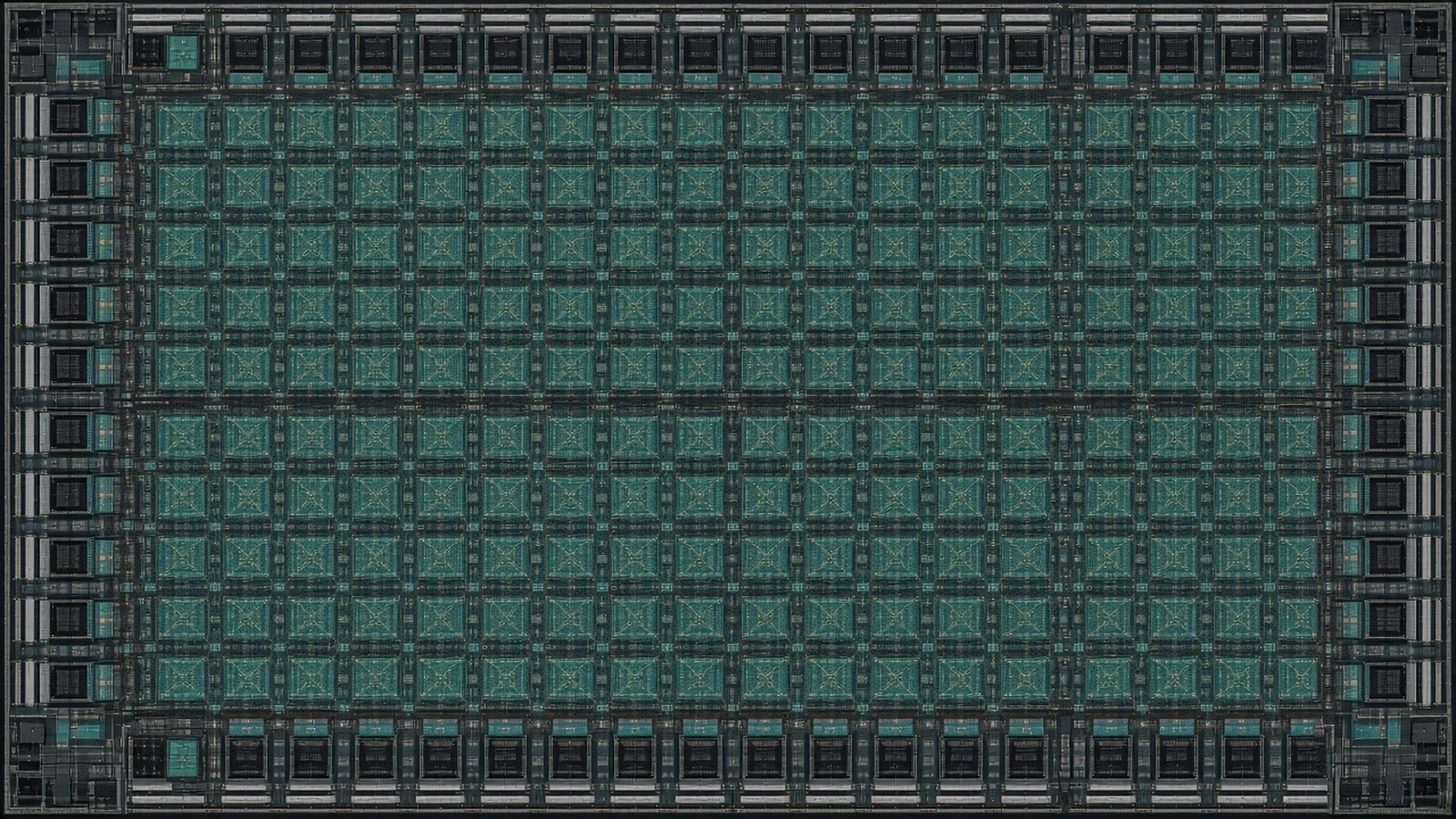
Silicon Showcase illustrative visual
Illustrative representation based on publicly available technical information.

STACKED DRAM CUBES

Stacked DRAM cubes on an advanced HBM base die

CURRENT SAMSUNG AI-MEMORY

Current Samsung AI-memory generation on the official HBM family page

APPLICATIONS

AI & HPC · Data Center

Public source

Samsung HBM4

Memory & Storage

Samsung HBM4 is a publicly named high-bandwidth memory device family for AI accelerators.

  • AI & HPC
  • Data Center
South KoreaView Official Source (opens in a new tab)

Silicon Showcase illustrative visual
Illustrative representation based on publicly available technical information.

Overview

Samsung HBM4 is the company’s current high-bandwidth DRAM stack for AI accelerators, with an advanced base die and stacked DRAM cubes. Samsung’s official HBM family page covers HBM3E through HBM4/HBM4E as the AI-memory roadmap.

Official Samsung Semiconductor pages present HBM as stacked DRAM cubes on an advanced base die, with HBM4 and HBM4E as the current AI-memory generation. This listing records Samsung’s HBM4 stack technology rather than every HBM generation. HBM3 and HBM3E remain prior generations of the same family rather than separate listings. Micron High-Bandwidth Memory and Synopsys HBM Interface IP, already in the catalog, are a different vendor’s device and a PHY/controller IP block. Capacity options and interface details should be taken from Samsung’s current HBM documentation.

Capabilities

Key characteristics associated with this technology.

  • Stacked DRAM cubes on an advanced HBM base die

  • Current Samsung AI-memory generation on the official HBM family page

  • Positioned for AI accelerator and data-center platforms

  • Distinct from Micron HBM devices and Synopsys HBM interface IP

Organization

Samsung Semiconductor

South Korea

View organization

Official resources

  • Samsung Semiconductor HBMsemiconductor.samsung.com (opens in a new tab)

Source & disclosure

Independent discovery listing. This profile was prepared from publicly available information published by the organization. For the latest and complete technical information, refer to the official company source.

Official source

semiconductor.samsung.com (opens in a new tab)

Last source check

Sep 15, 2026

Notice something that needs updating?

Report a correction

Related Technologies

Explore other semiconductor technologies.
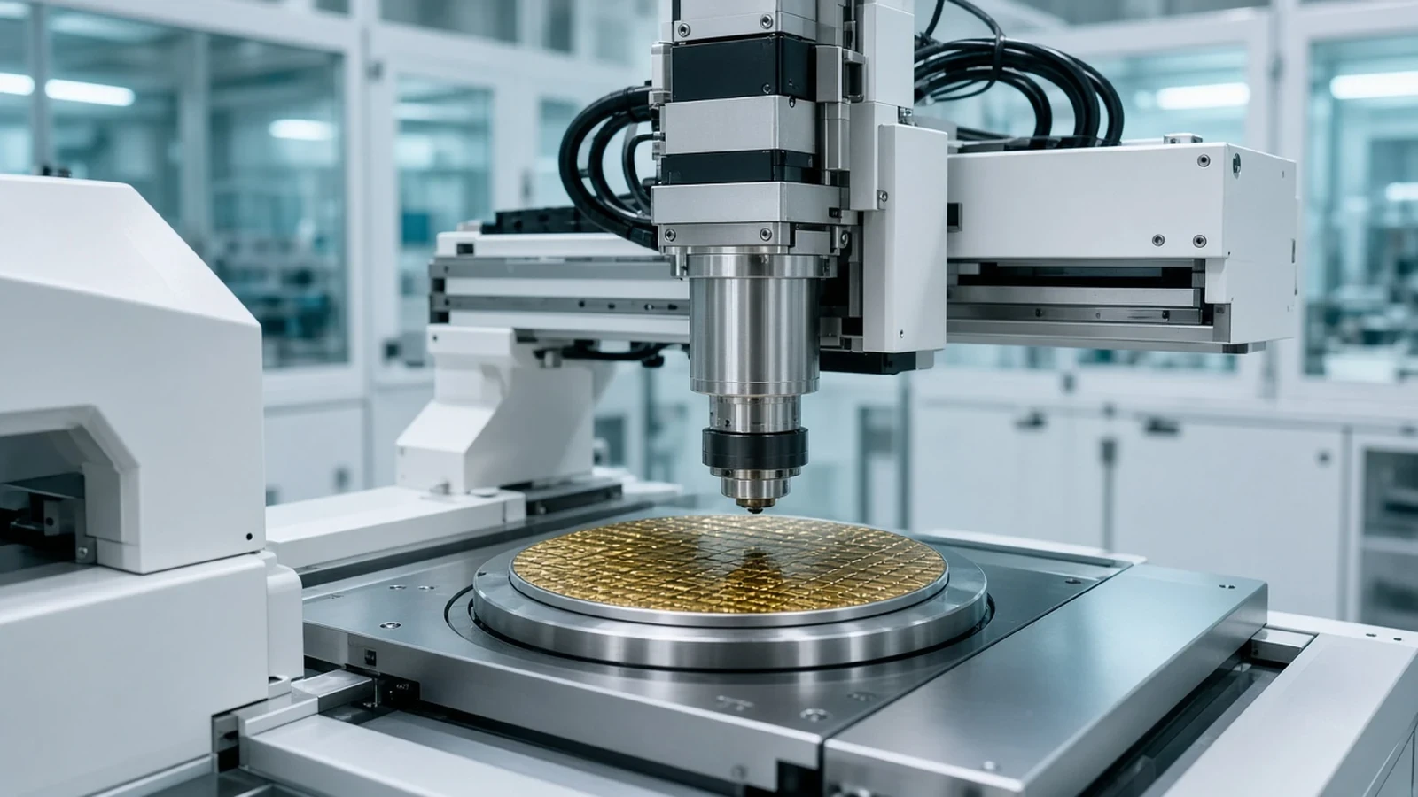
Advanced Packaging

APTURA Thermo-Compression Bonding

Kulicke & Soffa APTURA is a thermo-compression bonder for advanced packaging, not a wire bonder catalog and not OSAT assembly.

AI & HPCData CenterView Technology
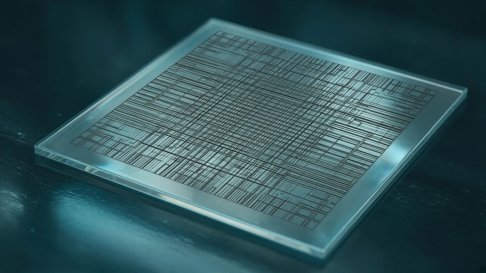
Materials & Substrates

Advanced IC Photomasks

Photronics advanced IC photomasks are lithography reticles for integrated circuits, not a foundry node and not FPD masks.

AutomotiveAI & HPCView Technology
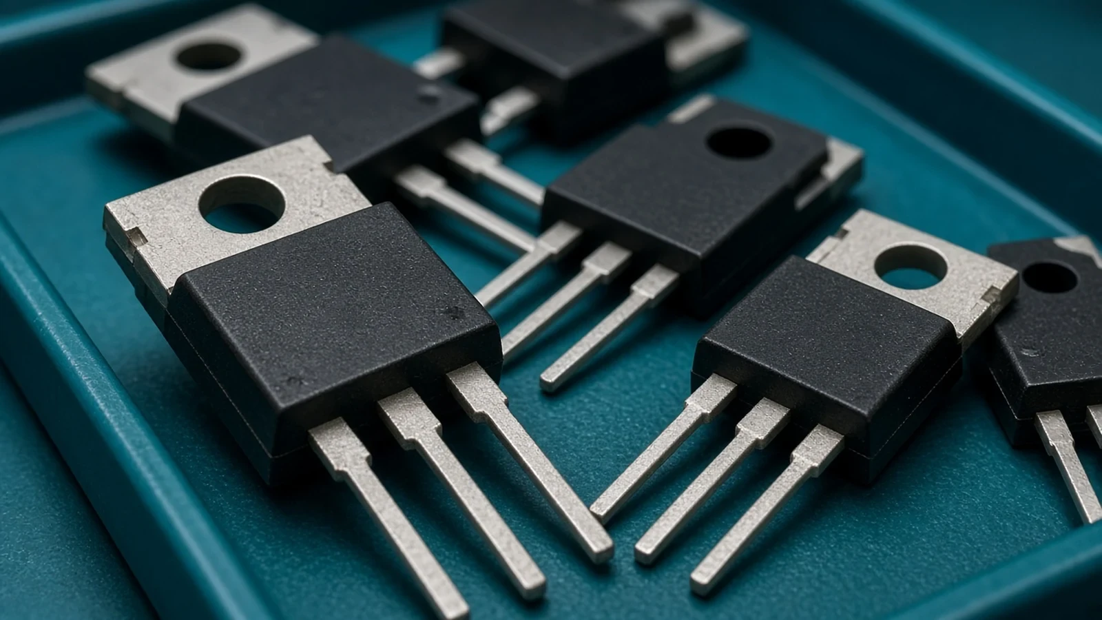
Power Semiconductors

AlphaSGT

AlphaSGT is Alpha and Omega’s shielded-gate trench MOSFET technology, not a GaN HEMT and not a power-module substrate.

AI & HPCData CenterView Technology
Design & IP

Australis eFPGA

QuickLogic Australis is embedded FPGA IP, not a standalone FPGA chip and not a foundry process.

AI & HPCIndustrialView Technology