Discover 169 technologies from leading innovators around the world.

Lightmatter Passage is a photonic interconnect platform using integrated photonics and three-dimensional connectivity approaches to scale high-bandwidth communication across advanced AI and computing systems.
AI & HPCData CenterView Technology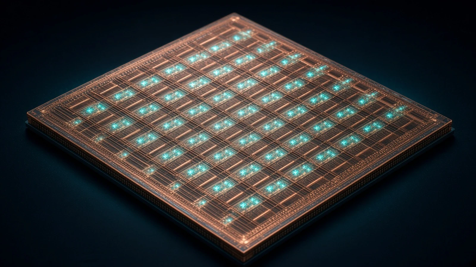
proteanTecs combines embedded on-chip monitoring agents and sensors with integration tools and analytics software to provide visibility into silicon performance, reliability and behavior across production and in-field operation.
AutomotiveAI & HPC+2View Technology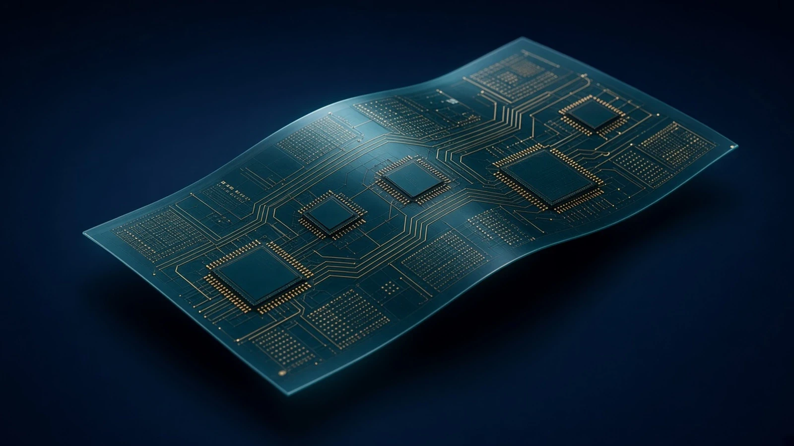
Pragmatic FlexIC Platform Gen 3 is a flexible semiconductor technology platform using metal-oxide thin-film transistors on flexible substrates for mixed-signal integrated circuits supporting connect, sense and basic compute functions.
IndustrialConsumer Electronics+1View Technology
Ayar Labs TeraPHY is an optical I/O chiplet that combines silicon photonics with CMOS technology to provide high-bandwidth, low-latency chip-to-chip and package-to-package connectivity for large-scale computing systems.
AI & HPCData Center+1View Technology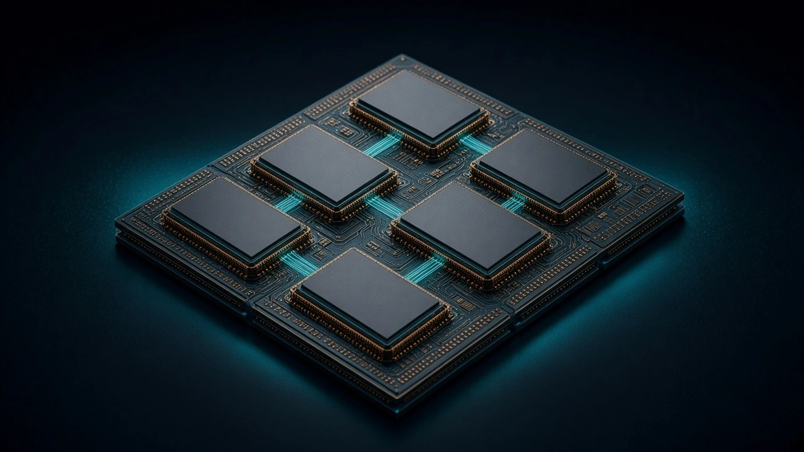
Arm Chiplet System Architecture provides standardized system partitioning and connectivity foundations for reusable chiplet-based designs. It is an architecture, not a processor-core catalog.
AutomotiveAI & HPC+1View Technology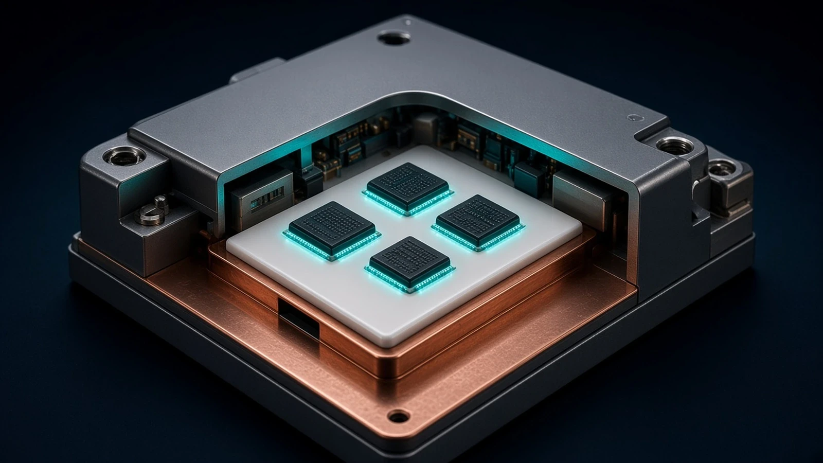
STPOWER silicon carbide MOSFET technology for high-voltage switching in automotive, industrial, energy and power-conversion systems. Distinct from STPOWER GaN.
AutomotiveData Center+2View Technology
ASM Atomic Layer Deposition technology enables highly controlled, layer-by-layer deposition of ultrathin conformal films for advanced semiconductor logic, memory and packaging structures.
AI & HPCData Center+1View Technology
Bosch MEMS sensor technology uses microelectromechanical structures to translate physical changes such as motion, pressure and environmental conditions into electrical information for compact sensing applications.
IndustrialConsumer Electronics+1View Technology
NVIDIA NVLink-C2C is a high-bandwidth coherent chip-to-chip interconnect for processors, accelerators and custom silicon inside a package. Distinct from NVLink GPU-to-GPU fabric.
AI & HPCData CenterView Technology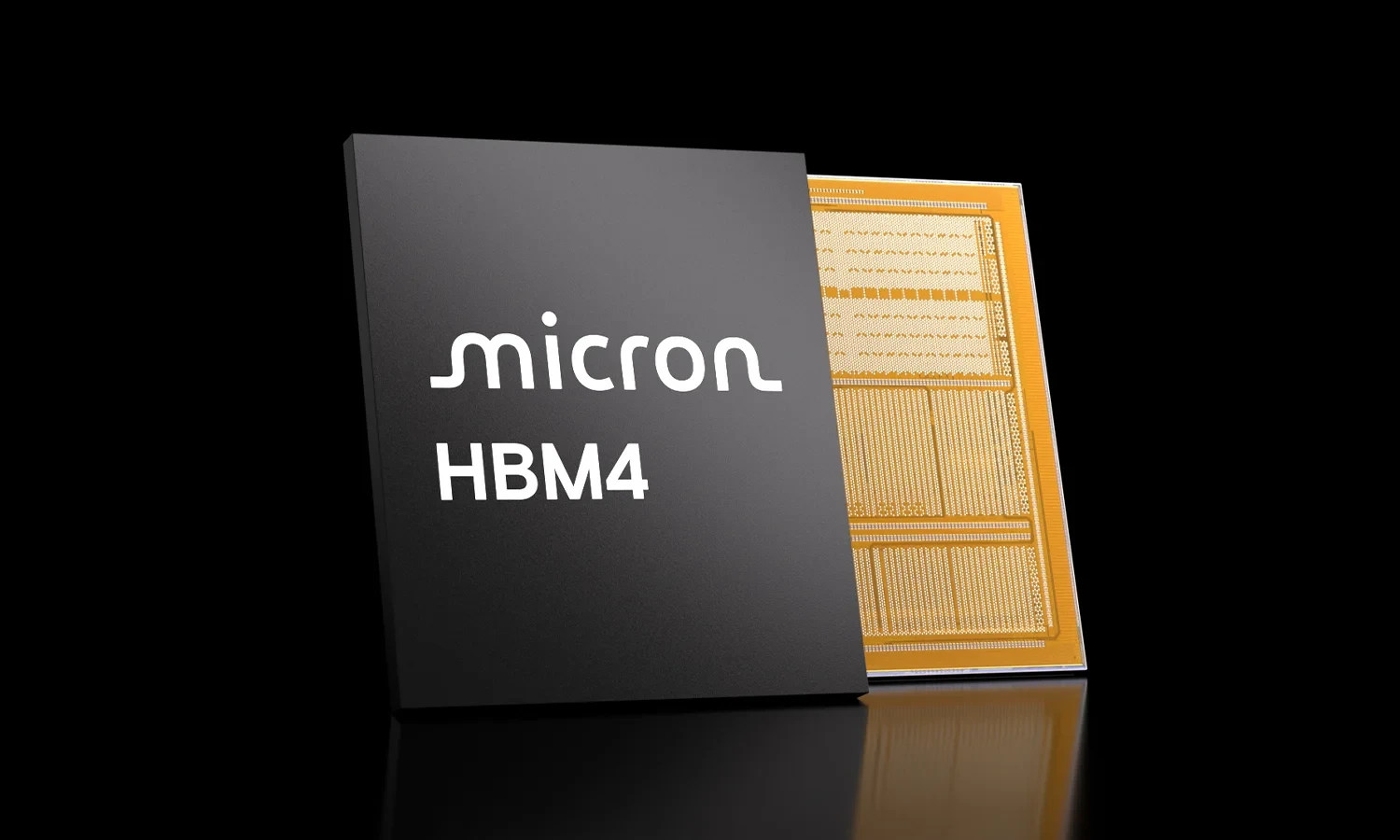
Micron high-bandwidth memory technology uses vertically stacked DRAM dies and high-density interconnects to provide high memory bandwidth and power efficiency for AI and data-center computing platforms.
AI & HPCData CenterView Technology
Microchip mSiC is a silicon carbide power semiconductor technology family spanning MOSFETs, Schottky barrier diodes, bare die and power modules. Those form factors are not separate listings.
AutomotiveData Center+3View Technology
Wolfspeed discrete silicon carbide MOSFET product line for power-conversion designs in industrial, energy and automotive systems.
AutomotiveIndustrial+1View Technology
imec silicon photonics platform family (iSiPP) for photonic integrated circuits. iSiPP200, iSiPP300 and related flavors are variants of this family, not separate listings.
Data CenterTelecommunicationsView Technology
Intel silicon photonics platform combining photonic integrated circuits and on-chip lasers for optical connectivity products. Optical compute interconnect remains part of this platform, not a separate listing.
Data CenterTelecommunicationsView Technology
KLA wafer defect inspection and review systems used to find, classify and monitor particles and pattern defects. Distinct from overlay and dimensional metrology.
AutomotiveData Center+1View Technology
Cadence design platform for planning, implementing and analyzing 2.5D and 3D multi-die / chiplet systems.
AutomotiveAI & HPC+1View Technology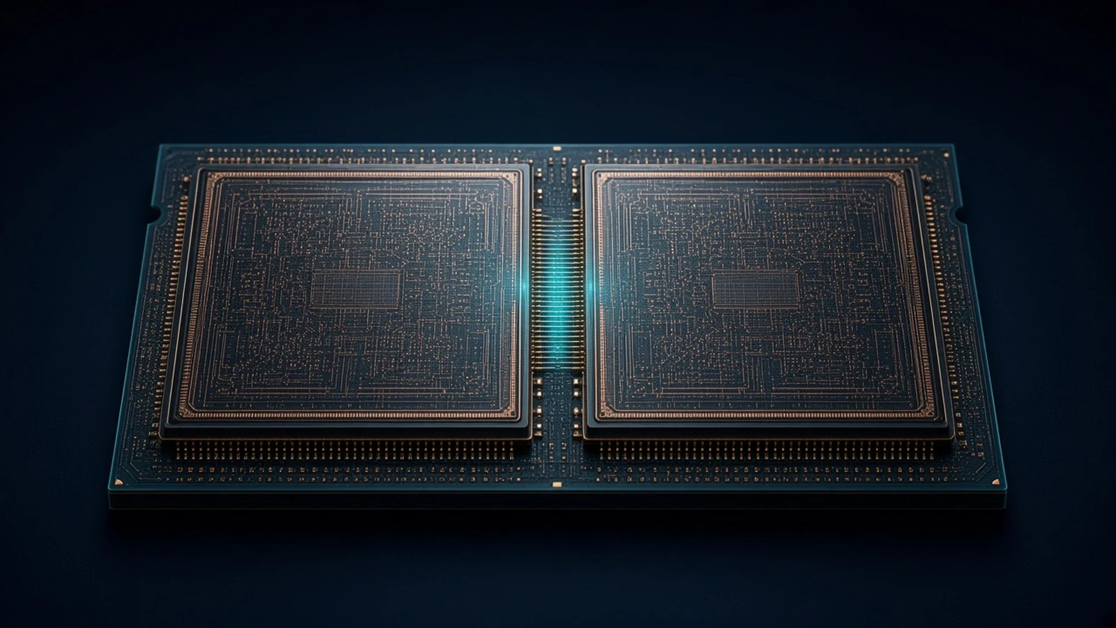
Synopsys die-to-die IP solution for Universal Chiplet Interconnect Express, including controller, PHY and verification IP.
AutomotiveAI & HPC+1View Technology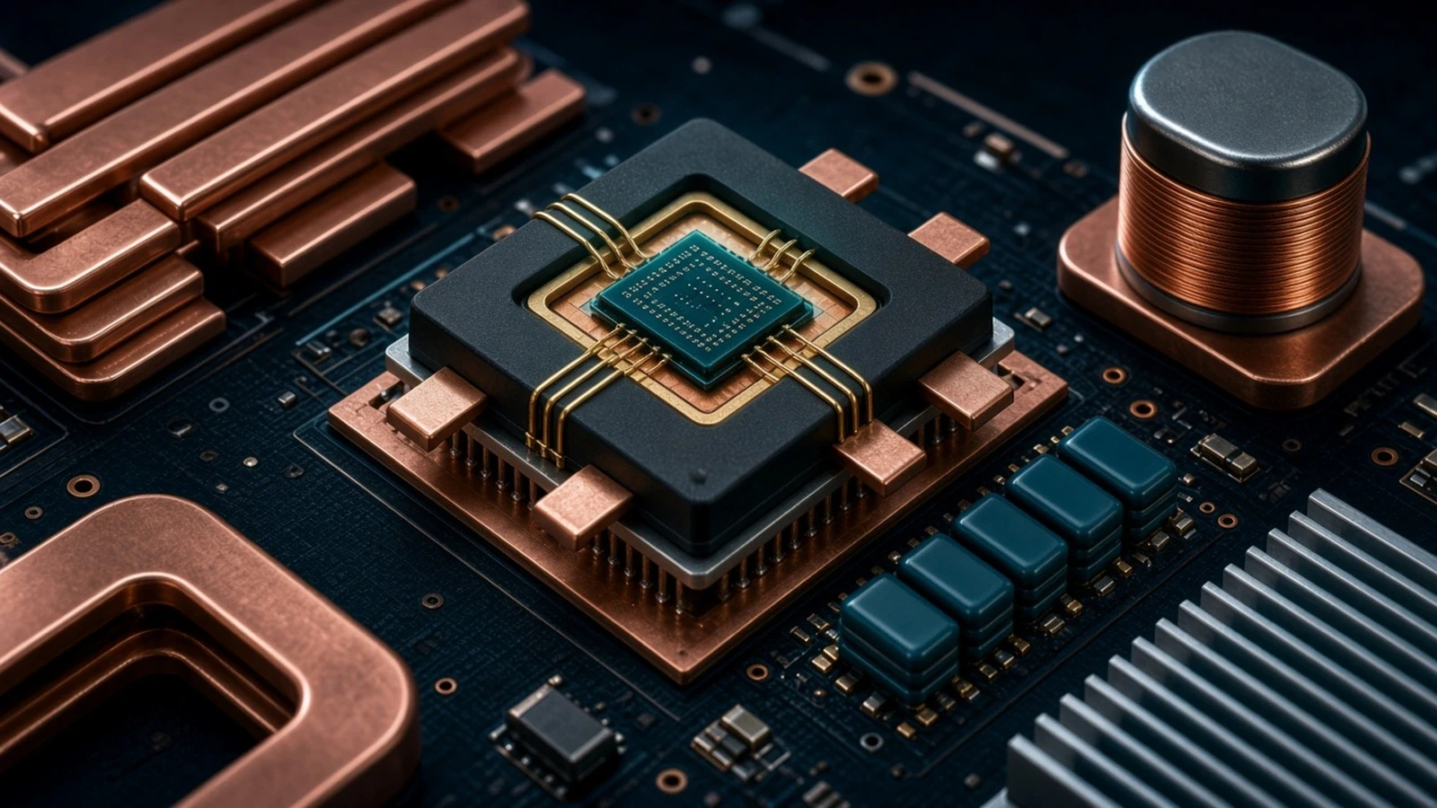
Infineon gallium nitride transistor family (CoolGaN) covering discrete and integrated normally-off GaN power devices.
Data CenterIndustrial+1View Technology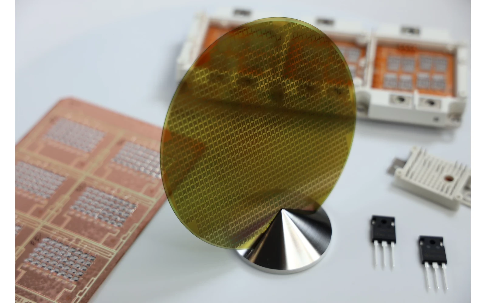
Infineon silicon carbide MOSFET family (CoolSiC) offered as discrete devices and power modules for power-conversion designs.
AutomotiveIndustrial+1View Technology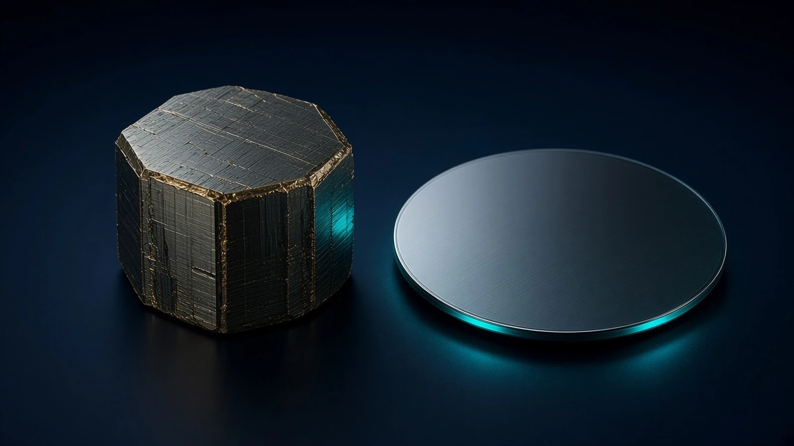
Wolfspeed conductive silicon carbide substrates and SiC epitaxy materials offered for power-electronics device manufacturing.
AutomotiveIndustrial+1View Technology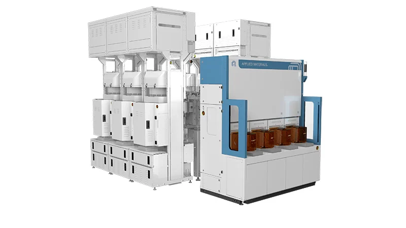
Modular semiconductor wafer-manufacturing chassis from Applied Materials for combining multiple chamber types on one system. Distinct from the Endura metallization platform.
AI & HPCData CenterView Technology
Lam Research wafer-process equipment category for thin-film deposition, plasma etch, strip, clean and related fabrication steps. SABRE ECD is listed separately.
Data CenterConsumer ElectronicsView Technology
ASML High-NA EUV lithography platform (TWINSCAN EXE) using 0.55 numerical aperture optics. Distinct from 0.33 NA TWINSCAN NXE EUV systems.
AI & HPCConsumer ElectronicsView Technology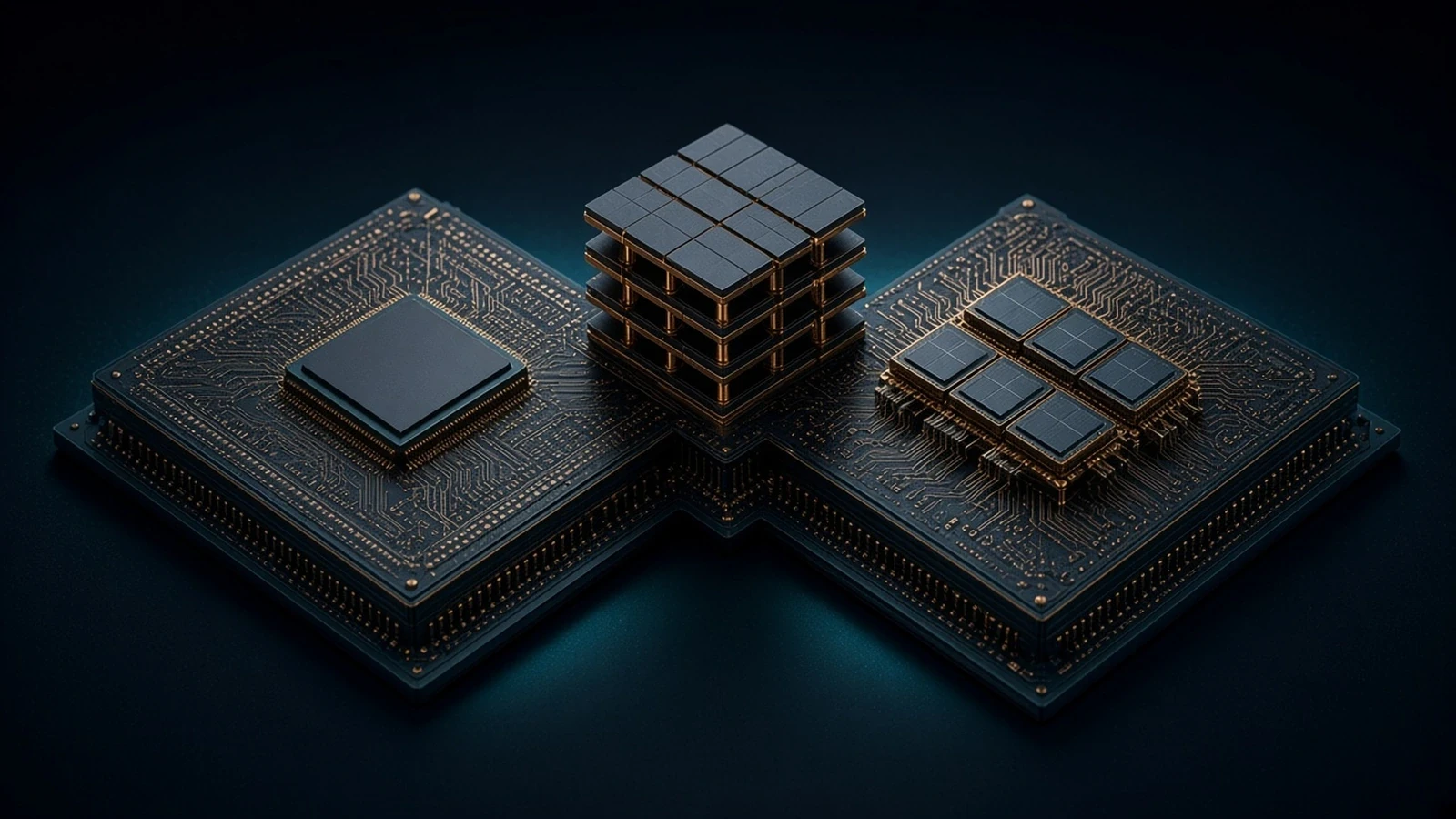
TSMC umbrella family of 3D silicon stacking and advanced packaging. CoWoS, TSMC-SoIC and InFO are constituent platforms listed separately.
AI & HPCData CenterView Technology