Emerging Signal
Chiplets, heterogeneous integration, hybrid bonding and 2.5D/3D packaging are increasingly becoming part of system architecture.
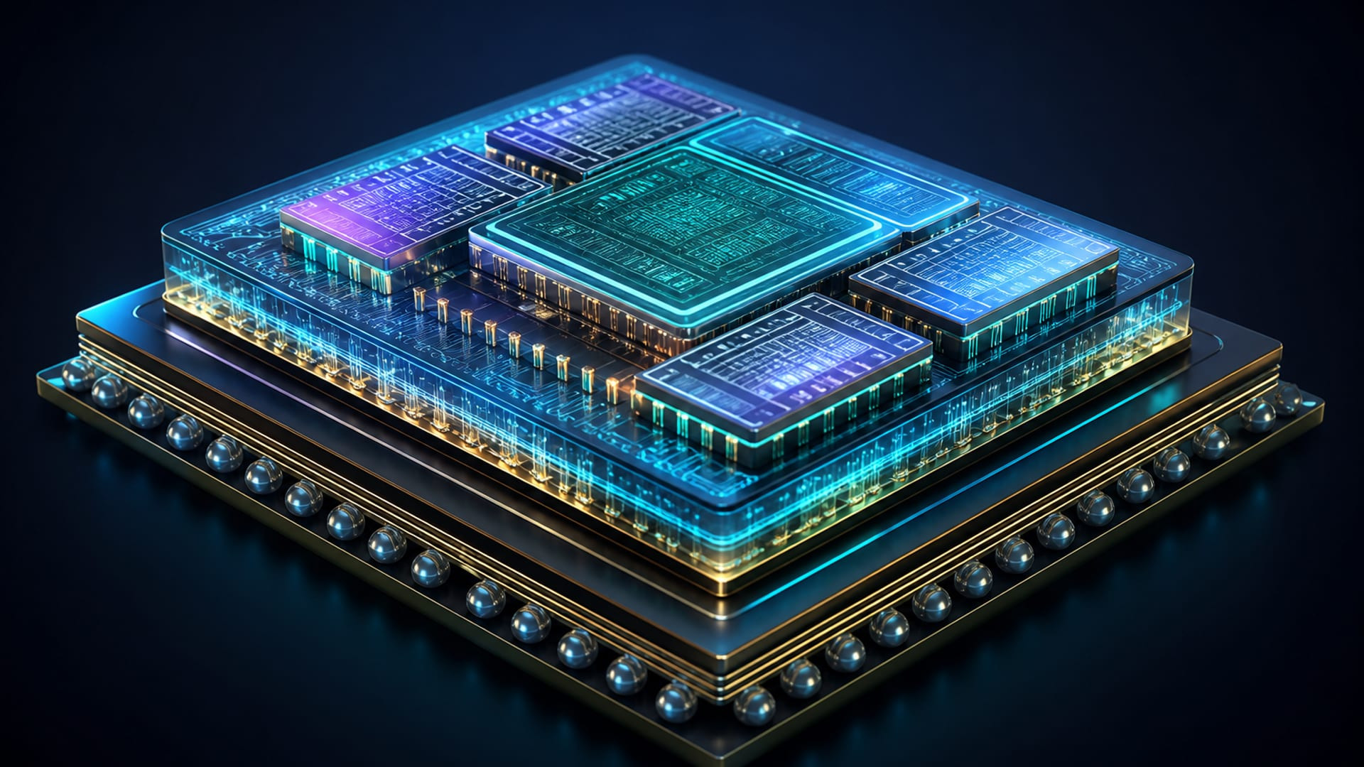
Advanced packaging now sits beside process-node choice as a way to combine logic, memory and I/O. 2.5D interposers, embedded bridges, fan-out and 3D stacking let designers assemble systems from chiplets rather than a single monolithic die.
AI and high-performance systems already depend on packaging to attach high-bandwidth memory and to connect heterogeneous dies. Architecture is no longer only a silicon-floorplan problem.
Watch 2.5D and 3D platform roadmaps, how chiplets are partitioned, and which interconnect and bonding methods foundries and IDMs standardize on.
United States2 technologies
Semiconductor company that publishes chiplet CPU architectures and 3D cache stacking, including Infinity Fabric and 3D V-Cache.
View ProfileUnited States3 technologies
Public semiconductor company that designs processors and related platforms and publishes foundry packaging, assembly and silicon photonics information for industry use.
View ProfileTaiwan4 technologies
Dedicated semiconductor foundry headquartered in Hsinchu, Taiwan, offering wafer manufacturing plus publicly described 3D stacking and advanced packaging services.
View Profile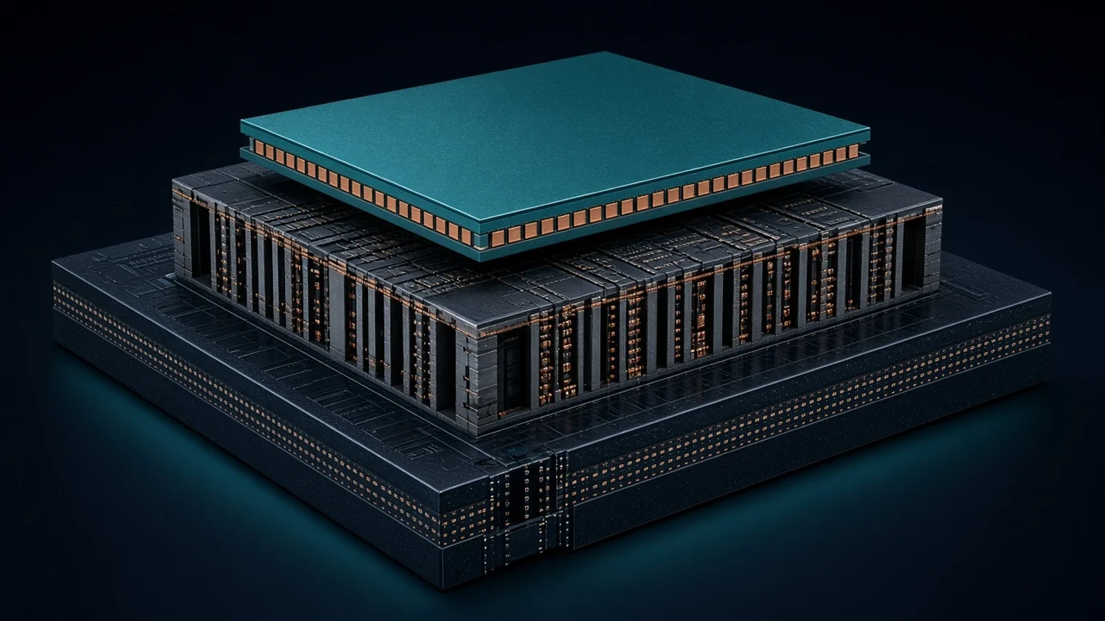
3D V-Cache stacks an L3 cache tile on a CPU core-complex die using copper-to-copper hybrid bonding and TSVs. Official AMD materials call it the first x86 true 3D die stack, with much higher interconnect density versus 2D chiplets.
AI & HPCData CenterView Technology
Intel EMIB is a 2.5D packaging technology that embeds a silicon interconnect bridge in the package substrate to connect neighboring dies without a full-size interposer.
AI & HPCData CenterView Technology
Intel Foundry 3D stacking and 2.5D chiplet packaging family, including hybrid-bonding options described as Foveros Direct 3D. EMIB is a separate 2.5D bridge platform.
AI & HPCData CenterView Technology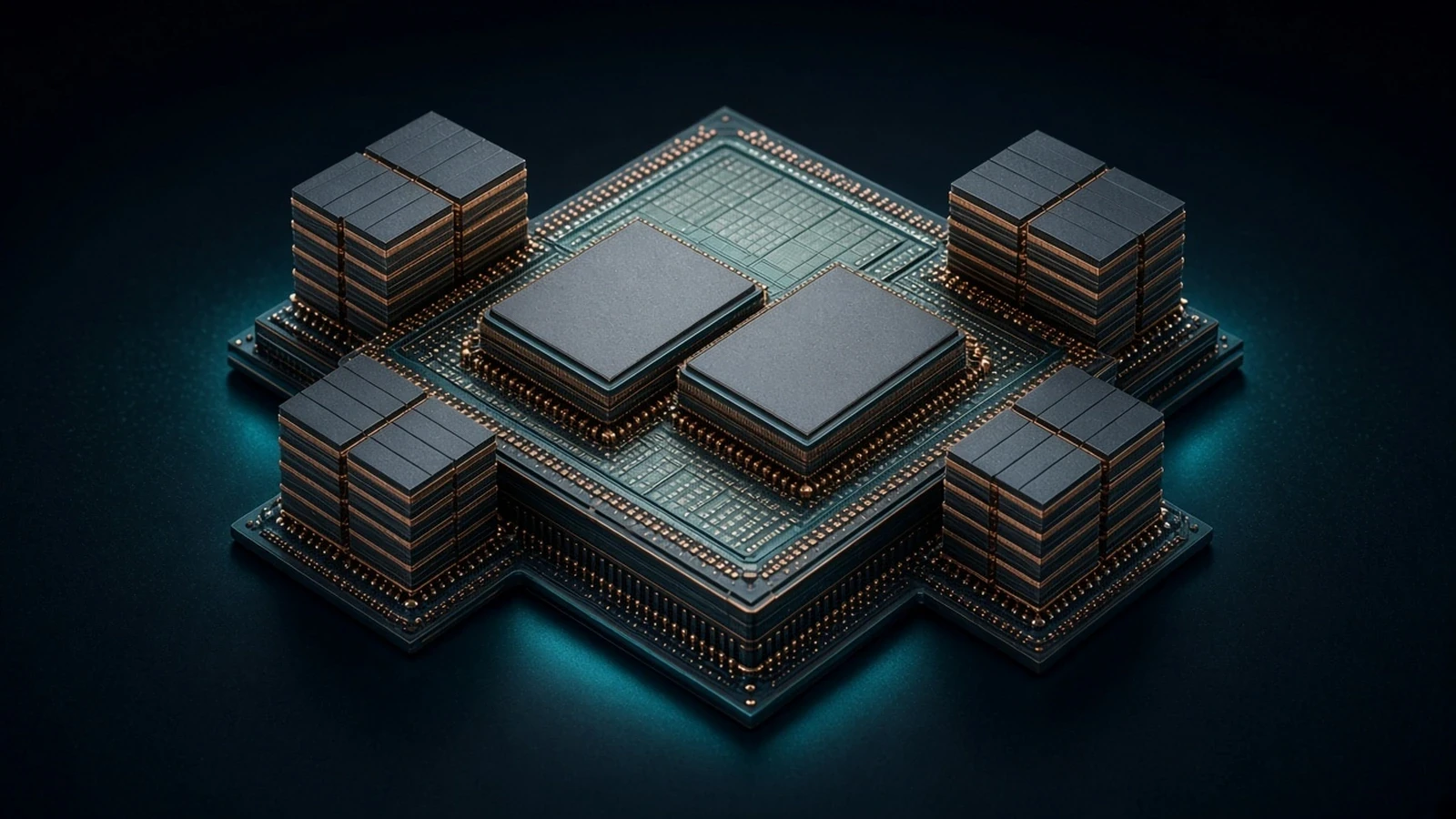
TSMC CoWoS is a 2.5D advanced packaging platform that integrates logic dies and high-bandwidth memory on an interposer for high-performance computing and AI systems.
AI & HPCData CenterView Technology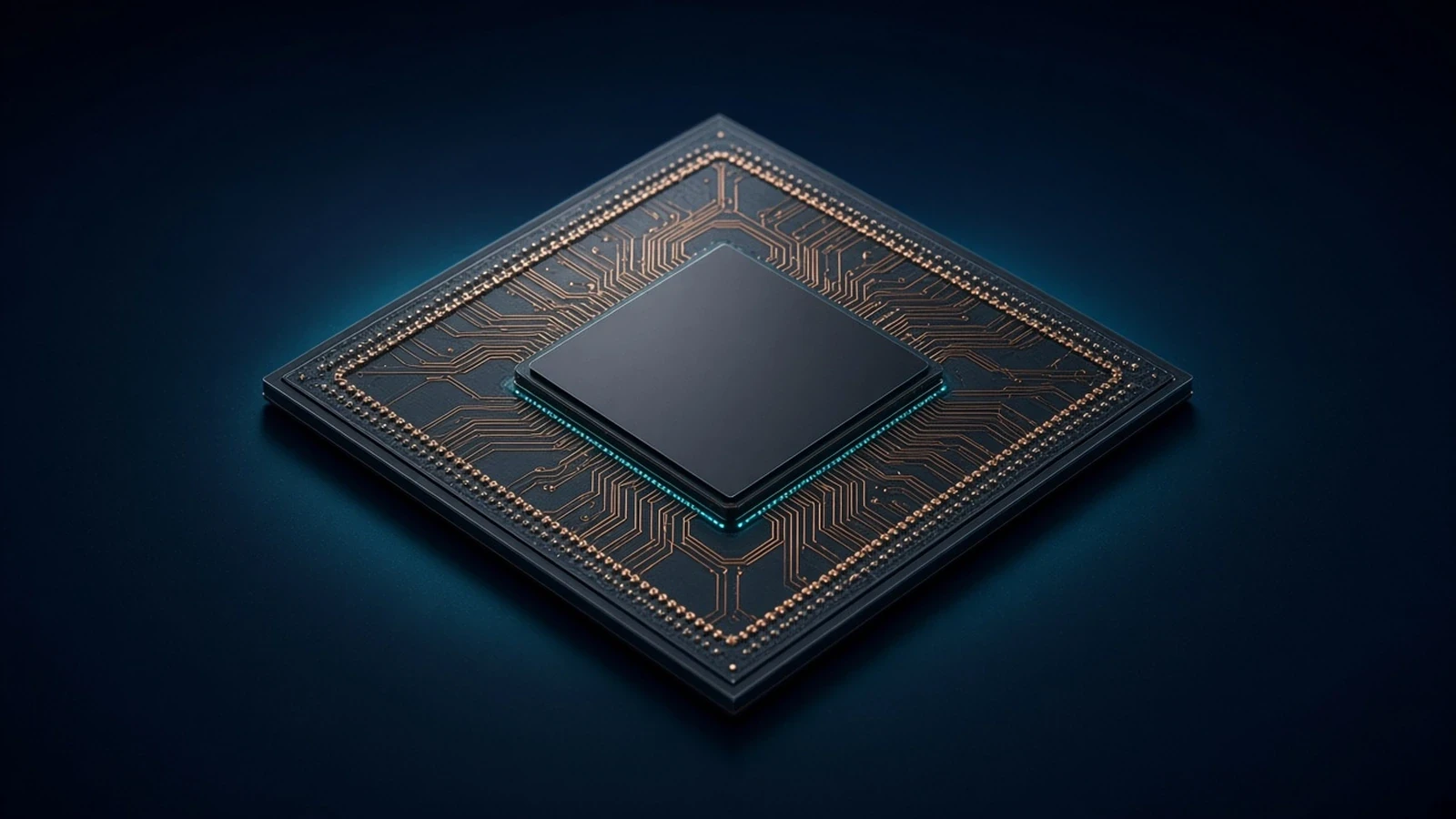
TSMC InFO is a wafer-level integrated fan-out packaging platform using high-density redistribution layers for mobile, network and high-performance computing integration.
AI & HPCConsumer ElectronicsView Technology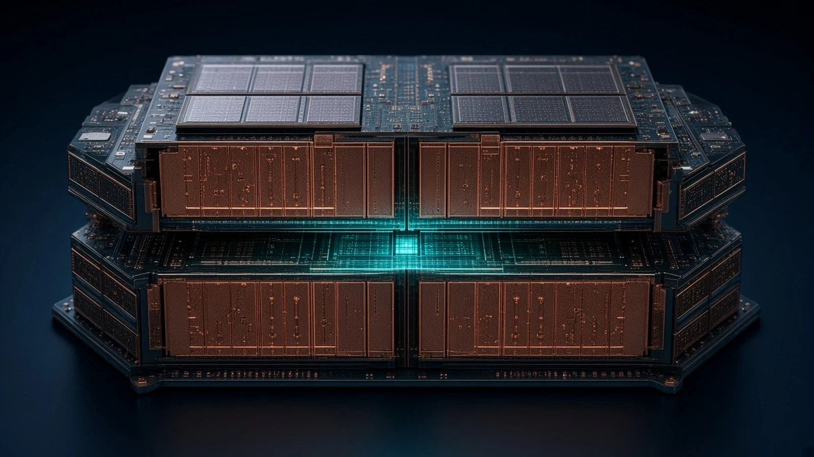
TSMC-SoIC is a wafer-level frontend 3D chip-stacking platform for homogeneous and heterogeneous chiplets, distinct from CoWoS 2.5D packaging and InFO fan-out.
AI & HPCData CenterView TechnologyTSMC · Primary
CoWoS
Visit source (opens in a new tab)TSMC
TSMC-SoIC
Visit source (opens in a new tab)Intel
Advanced Packaging Innovations
Visit source (opens in a new tab)Technology Signals are editorial summaries based on publicly available sources. Technical claims remain attributable to their original sources.