Skip to content
Silicon Showcase
CompaniesApplicationsTechnology AreasAbout
Submit Technology
Submit Technology
Silicon Showcase

Silicon Showcase™ is the global directory of semiconductor technologies, platforms and innovations from around the world.

  • Technologies
  • Technology Signals
  • Companies
  • Applications
  • Technology Areas
  • About Us
  • How It Works
  • Submit Technology
  • Contact Us
  • Privacy Policy
  • Terms of Use
  • Disclaimer

Explore

  • Technologies
  • Technology Signals
  • Companies
  • Applications
  • Technology Areas

About

  • About Us
  • How It Works
  • Submit Technology
  • Contact Us

Legal

  • Privacy Policy
  • Terms of Use
  • Disclaimer

© 2026 Silicon Showcase™. All rights reserved.

Explore. Compare. Innovate.

Silicon Showcase
CompaniesApplicationsTechnology AreasAbout
Submit Technology
Submit Technology
Silicon Showcase

Silicon Showcase™ is the global directory of semiconductor technologies, platforms and innovations from around the world.

  • Technologies
  • Technology Signals
  • Companies
  • Applications
  • Technology Areas
  • About Us
  • How It Works
  • Submit Technology
  • Contact Us
  • Privacy Policy
  • Terms of Use
  • Disclaimer

Explore

  • Technologies
  • Technology Signals
  • Companies
  • Applications
  • Technology Areas

About

  • About Us
  • How It Works
  • Submit Technology
  • Contact Us

Legal

  • Privacy Policy
  • Terms of Use
  • Disclaimer

© 2026 Silicon Showcase™. All rights reserved.

Explore. Compare. Innovate.

  1. Home
  2. /Technology Areas
  3. /Advanced Packaging

Technology Area

Advanced Packaging

Heterogeneous integration, 2.5D/3D stacking, bonding and chiplet assembly approaches.

Technologies

12

Technologies

Companies

8

Companies

Applications

4

Applications

About Advanced Packaging

Advanced packaging brings together multiple dies, chiplets and components into integrated systems, enabling higher performance, improved power efficiency and new form factors. It includes 2.5D/3D integration, interposers, hybrid bonding, chiplet ecosystems and heterogeneous integration approaches that extend beyond traditional scaling.

Key Segments

  • 2.5D / 3D Integration
  • Chiplets & Heterogeneous Integration
  • Interposers & Bridges
  • Advanced Bonding
  • System-in-Package (SiP)

Why It Matters

  • Higher performance
  • Greater integration density
  • Improved power efficiency
  • Smaller system footprints

Explore Technologies

Discover technologies, solutions and innovations in this area.
View all technologies
Advanced Packaging

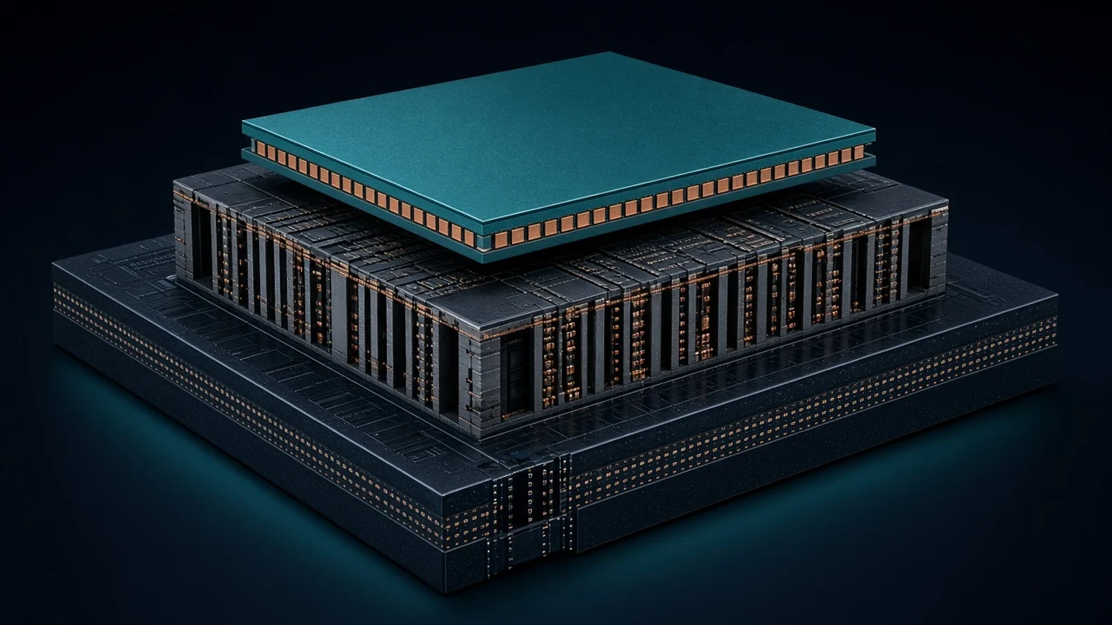
AMD 3D V-Cache

3D V-Cache stacks an L3 cache tile on a CPU core-complex die using copper-to-copper hybrid bonding and TSVs. Official AMD materials call it the first x86 true 3D die stack, with much higher interconnect density versus 2D chiplets.

AI & HPCData CenterConsumer ElectronicsView Technology
Advanced Packaging

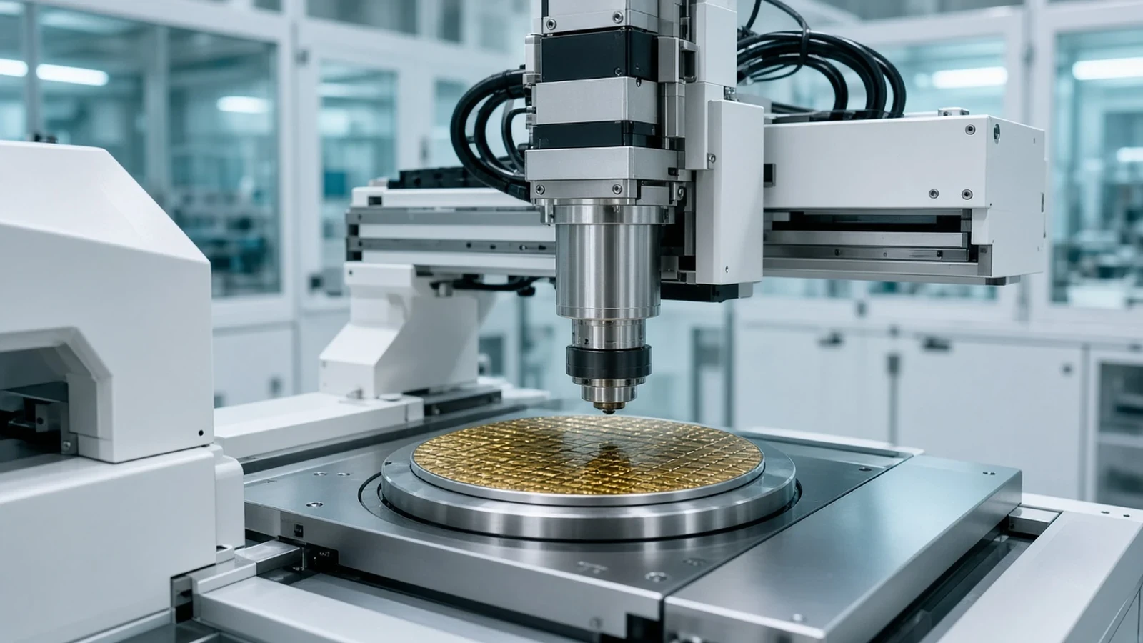
APTURA Thermo-Compression Bonding

Kulicke & Soffa APTURA is a thermo-compression bonder for advanced packaging, not a wire bonder catalog and not OSAT assembly.

AI & HPCData CenterConsumer ElectronicsView Technology
Advanced Packaging

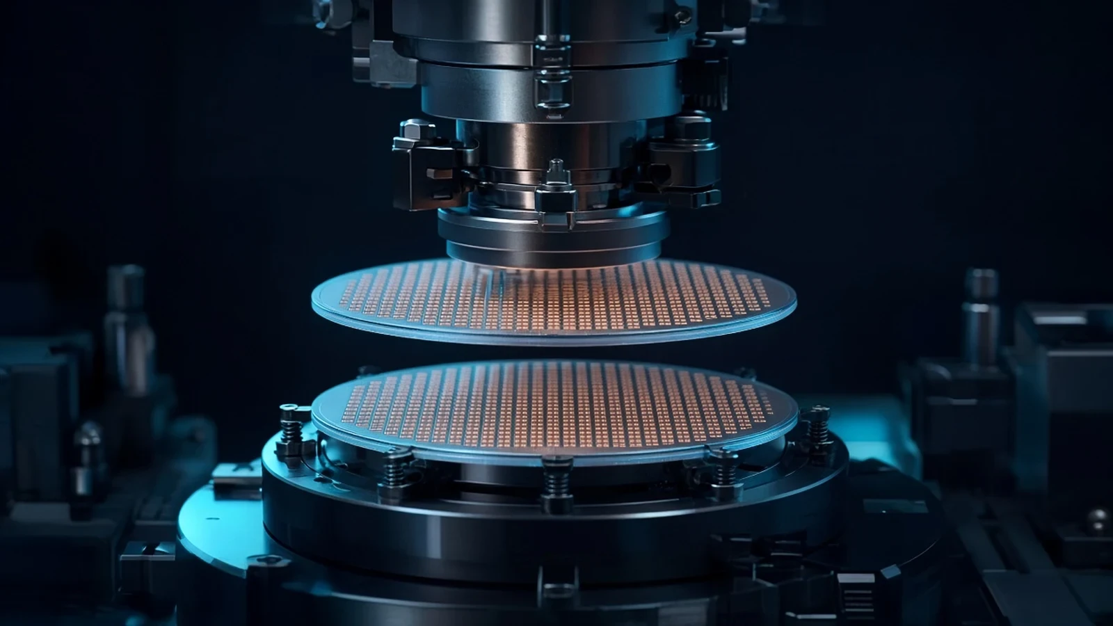
Datacon 8800 CHAMEO Hybrid Bonding

Besi Datacon 8800 CHAMEO is a hybrid-bonding die-attach platform for copper-to-copper and related advanced-package construction.

AI & HPCData CenterConsumer ElectronicsView Technology

Related Applications

Key application areas leveraging these technologies.

View all applications
AI & HPCData CenterConsumer ElectronicsTelecommunications

Technology area visuals are illustrative representations.