Discover 169 technologies from leading innovators around the world.
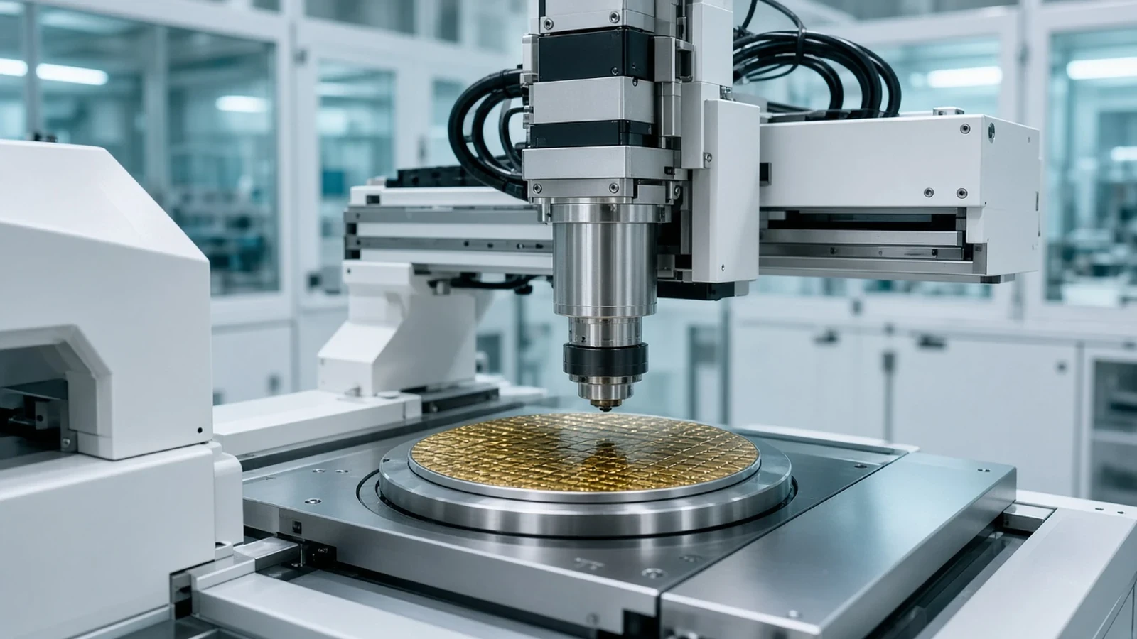
Kulicke & Soffa APTURA is a thermo-compression bonder for advanced packaging, not a wire bonder catalog and not OSAT assembly.
AI & HPCData CenterConsumer ElectronicsView Technology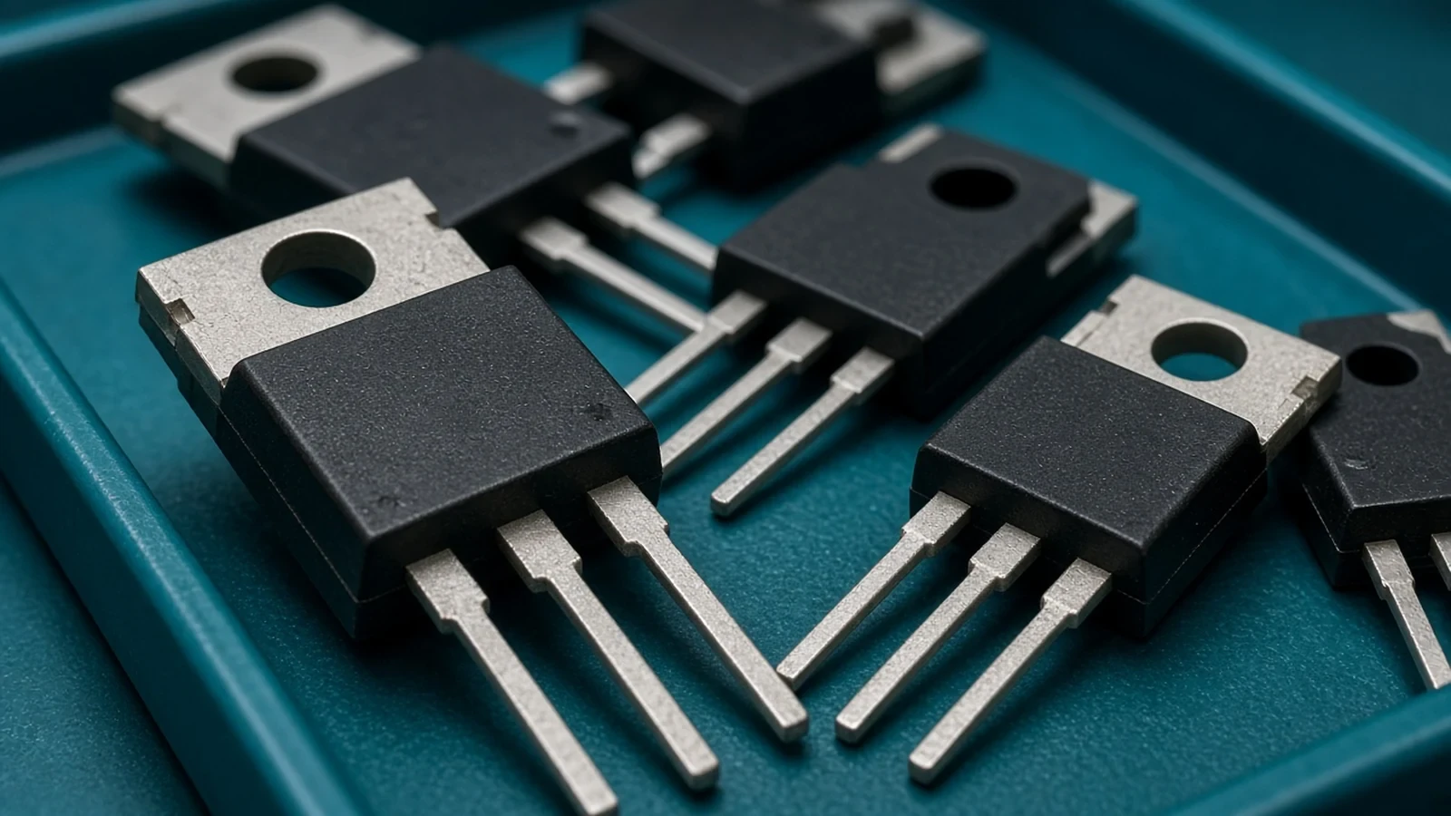
AlphaSGT is Alpha and Omega’s shielded-gate trench MOSFET technology, not a GaN HEMT and not a power-module substrate.
AI & HPCData CenterIndustrialView Technology
Arteris FlexNoC is on-chip network IP, not a packaged interconnect chip and not a coherent cache controller.
AutomotiveAI & HPCData CenterView Technology
AXT VGF substrates are III-V wafers grown by vertical gradient freeze, not epiwafers and not finished RF chips.
Data CenterTelecommunicationsAerospace & DefenseView Technology
GUC APT is a 2.5D/3D multi-die ASIC packaging-design platform, not a foundry process node and not OSAT assembly.
AI & HPCData CenterTelecommunicationsView Technology
Powerchip 3D AI Foundry is a wafer-on-wafer logic/memory stacking foundry offering, parked in Advanced Packaging because Foundry / Process does not yet exist.
AutomotiveAI & HPCData CenterView Technology
Kokusai Batch ALD combines atomic-layer deposition with multi-wafer batch furnaces for 3D device films.
AI & HPCData CenterConsumer ElectronicsView Technology
FormFactor composite-metal MEMS is a wafer-probe-card technology, not a MEMS sensor product.
AutomotiveAI & HPCData CenterView Technology
Camtek Eagle is a wafer inspection and metrology equipment platform for BEOL, advanced packaging and related flows.
AutomotiveAI & HPCData CenterView Technology
Rohm EcoGaN is a gallium-nitride power-device family, not a silicon MOSFET catalog.
AutomotiveData CenterIndustrial+1View Technology
Qnity Emblem is a next-generation CMP pad platform for advanced-node planarization, not a polishing tool.
AI & HPCData CenterConsumer ElectronicsView Technology
Realtek Ethernet Total Solutions is a wired-connectivity PHY and controller platform, currently evidenced by live 2.5GbE product pages.
Data CenterConsumer ElectronicsTelecommunications+1
MACOM’s European Semiconductor Center publishes GaAs and GaN III-V foundry processes for microwave and mmWave devices.
Data CenterTelecommunicationsAerospace & DefenseView Technology
Silergy’s integrated PMIC platform covers multi-rail power-management ICs, not discrete MOSFETs.
AutomotiveData CenterIndustrial+1View Technology
ASMPT LITHOBOLT G2 is a die-to-wafer hybrid-bonding system for direct and collective bonding.
AutomotiveAI & HPCData CenterView Technology
SiTime MEMS First and EpiSeal are resonator fabrication processes that encapsulate silicon MEMS in epitaxial vacuum cavities.
AutomotiveData CenterTelecommunications+1View Technology
Nova’s multidisciplinary metrology platform combines optical scatterometry, X-ray and materials analysis for process control.
AutomotiveAI & HPCData CenterView Technology
Aixtron Planetary Reactor is a batch MOCVD reactor architecture for compound-semiconductor epitaxy.
AutomotiveData CenterTelecommunications+1View Technology
SUMCO Advanced Silicon Wafers are polished and specialty silicon starting substrates, including epitaxial, annealed and SOI wafers.
AutomotiveAI & HPCData Center+1View Technology
ACM Ultra C is a wet-clean and wet-process equipment family, not an IR homepage listing.
AutomotiveAI & HPCData CenterView Technology
Alchip’s 2nm Design Platform is an ASIC physical-design methodology for 2nm compute dies and chiplet packaging, not a foundry process node.
AI & HPCData CenterTelecommunicationsView Technology
The Dragonfly G5 System is Onto Innovation's advanced-packaging inspection and metrology system.
AutomotiveAI & HPCData CenterView Technology
AT&S high-performance IC substrates are build-up package substrates that connect advanced processors to system boards, not generic PCBs and not OSAT assembly.
AutomotiveAI & HPCData Center+1View Technology
Coherent’s III-V epitaxial wafer platform supplies compound-semiconductor epi wafers for photonic and RF devices, not industrial laser systems.
AutomotiveData CenterIndustrial+1View Technology