Discover 169 technologies from leading innovators around the world.
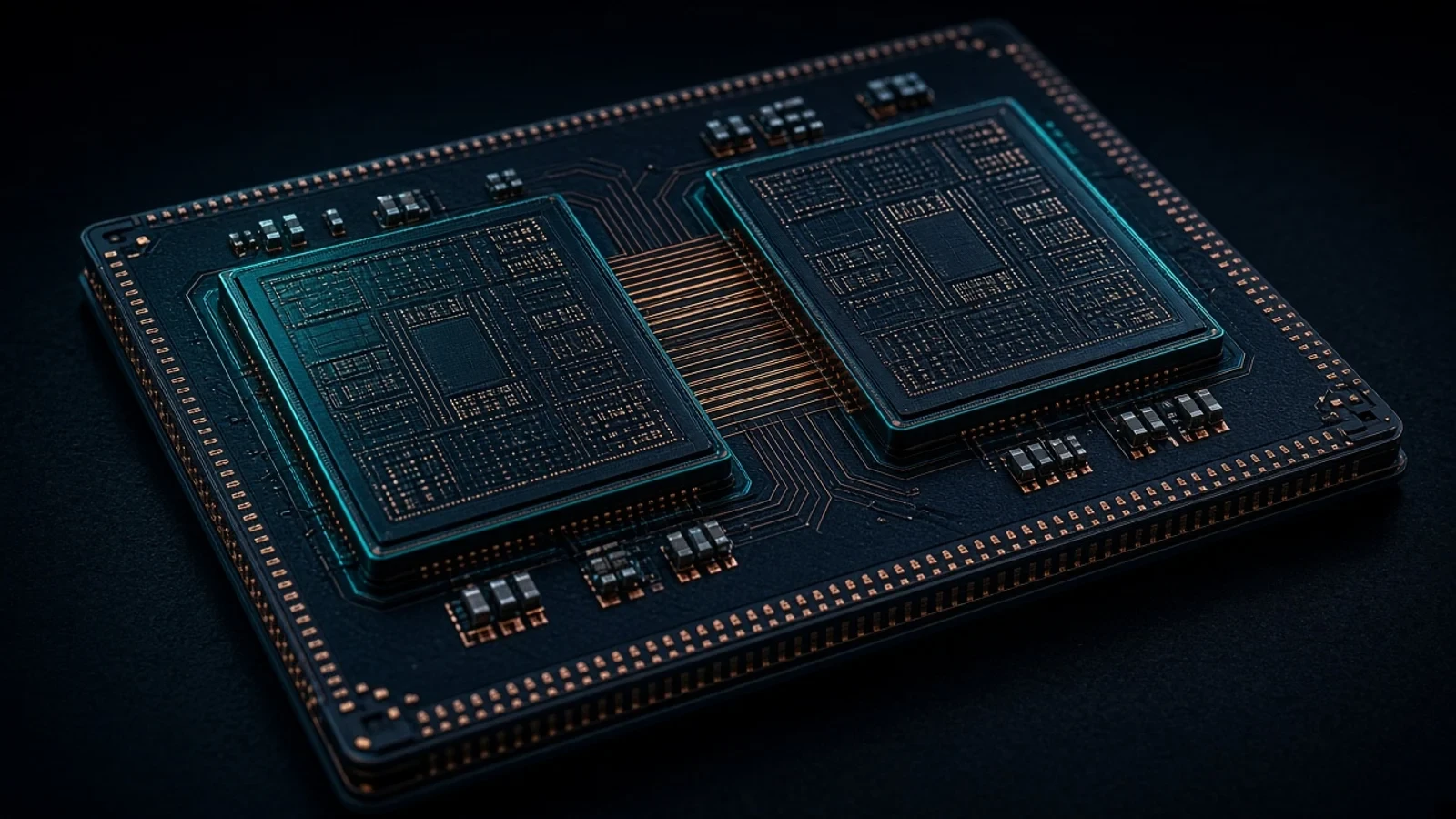
TPU7x (Ironwood) is Google Cloud's seventh-generation TPU, built for large-scale training and inference.
AI & HPCData CenterView Technology
Micron DDR DRAM is a synchronous DRAM component family spanning successive double-data-rate generations for data-center, industrial and automotive designs.
AutomotiveData Center+1View Technology
Micron 3D NAND is a vertically stacked NAND flash technology family used as the semiconductor storage building block in data-center, client, mobile and automotive designs.
AutomotiveAI & HPC+2View Technology
Micron LPDDR is a low-power DRAM family for mobile, client, automotive and data-center designs that need high bandwidth at reduced power. LPDDR generations remain one technology line.
AutomotiveAI & HPC+2View Technology
Micron GDDR is a discrete graphics DRAM family spanning GDDR6, GDDR6X and GDDR7 generations for GPUs, gaming systems and AI inference accelerators.
AI & HPCConsumer ElectronicsView Technology
Microchip PolarFire SoC combines a coherent multi-core RISC-V CPU subsystem with PolarFire FPGA fabric on one device for Linux and real-time embedded systems.
IndustrialMedical+2View Technology
Microchip PolarFire is a mid-range FPGA family providing programmable logic fabric, optional high-speed serial transceivers and on-chip interface IP for communications, imaging and embedded systems.
IndustrialMedical+2View Technology
Lam Research SABRE is an electrochemical copper-deposition platform for damascene interconnect, including logic, memory and high-bandwidth memory wiring. Distinct from Lam’s broader etch category.
AI & HPCData CenterView Technology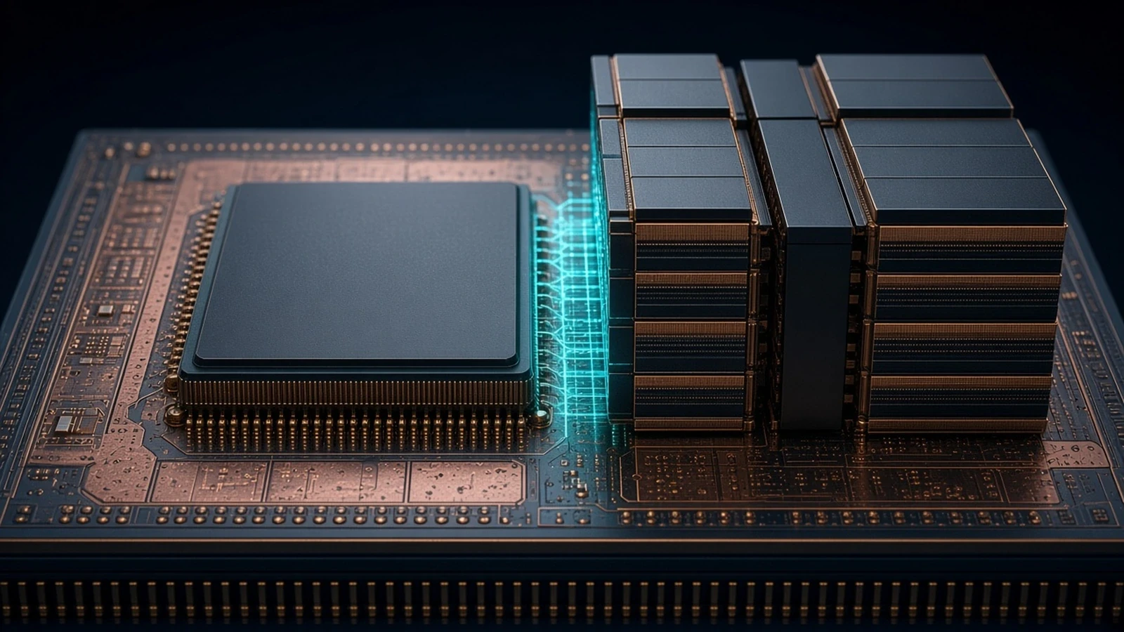
Synopsys HBM interface IP is a high-bandwidth memory interface family including controller, PHY and verification IP for AI and high-performance computing SoCs. Distinct from UCIe die-to-die IP.
AI & HPCData CenterView Technology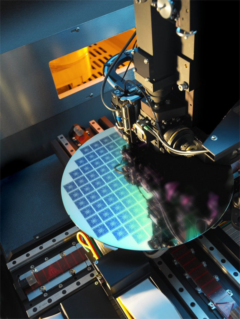
KLA overlay and dimensional metrology systems measure layer-to-layer alignment, critical dimensions and related pattern geometry. Distinct from defect inspection and review.
AutomotiveData Center+1View Technology
Applied Materials Endura is an ultra-high-vacuum metallization platform used for physical vapor deposition and integrated multi-chamber sequences. Distinct from the Vistara wafer-manufacturing chassis.
AI & HPCData CenterView Technology
NVIDIA NVLink is a high-bandwidth GPU-to-GPU interconnect and rack-scale fabric for AI training and inference. Distinct from NVLink-C2C chip-to-chip packaging links.
AI & HPCData CenterView Technology
Intel EMIB is a 2.5D packaging technology that embeds a silicon interconnect bridge in the package substrate to connect neighboring dies without a full-size interposer.
AI & HPCData CenterView Technology
Lightmatter Passage is a photonic interconnect platform using integrated photonics and three-dimensional connectivity approaches to scale high-bandwidth communication across advanced AI and computing systems.
AI & HPCData CenterView Technology
Ayar Labs TeraPHY is an optical I/O chiplet that combines silicon photonics with CMOS technology to provide high-bandwidth, low-latency chip-to-chip and package-to-package connectivity for large-scale computing systems.
AI & HPCData Center+1View Technology
NVIDIA NVLink-C2C is a high-bandwidth coherent chip-to-chip interconnect for processors, accelerators and custom silicon inside a package. Distinct from NVLink GPU-to-GPU fabric.
AI & HPCData CenterView Technology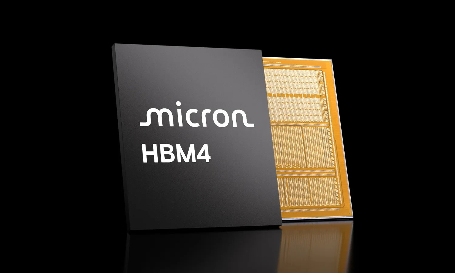
Micron high-bandwidth memory technology uses vertically stacked DRAM dies and high-density interconnects to provide high memory bandwidth and power efficiency for AI and data-center computing platforms.
AI & HPCData CenterView Technology
Microchip mSiC is a silicon carbide power semiconductor technology family spanning MOSFETs, Schottky barrier diodes, bare die and power modules. Those form factors are not separate listings.
AutomotiveData Center+3View Technology
Wolfspeed discrete silicon carbide MOSFET product line for power-conversion designs in industrial, energy and automotive systems.
AutomotiveIndustrial+1View Technology
Intel silicon photonics platform combining photonic integrated circuits and on-chip lasers for optical connectivity products. Optical compute interconnect remains part of this platform, not a separate listing.
Data CenterTelecommunicationsView Technology
KLA wafer defect inspection and review systems used to find, classify and monitor particles and pattern defects. Distinct from overlay and dimensional metrology.
AutomotiveData Center+1View Technology
Cadence design platform for planning, implementing and analyzing 2.5D and 3D multi-die / chiplet systems.
AutomotiveAI & HPC+1View Technology
Synopsys die-to-die IP solution for Universal Chiplet Interconnect Express, including controller, PHY and verification IP.
AutomotiveAI & HPC+1View Technology
Wolfspeed conductive silicon carbide substrates and SiC epitaxy materials offered for power-electronics device manufacturing.
AutomotiveIndustrial+1View Technology