Discover 169 technologies from leading innovators around the world.
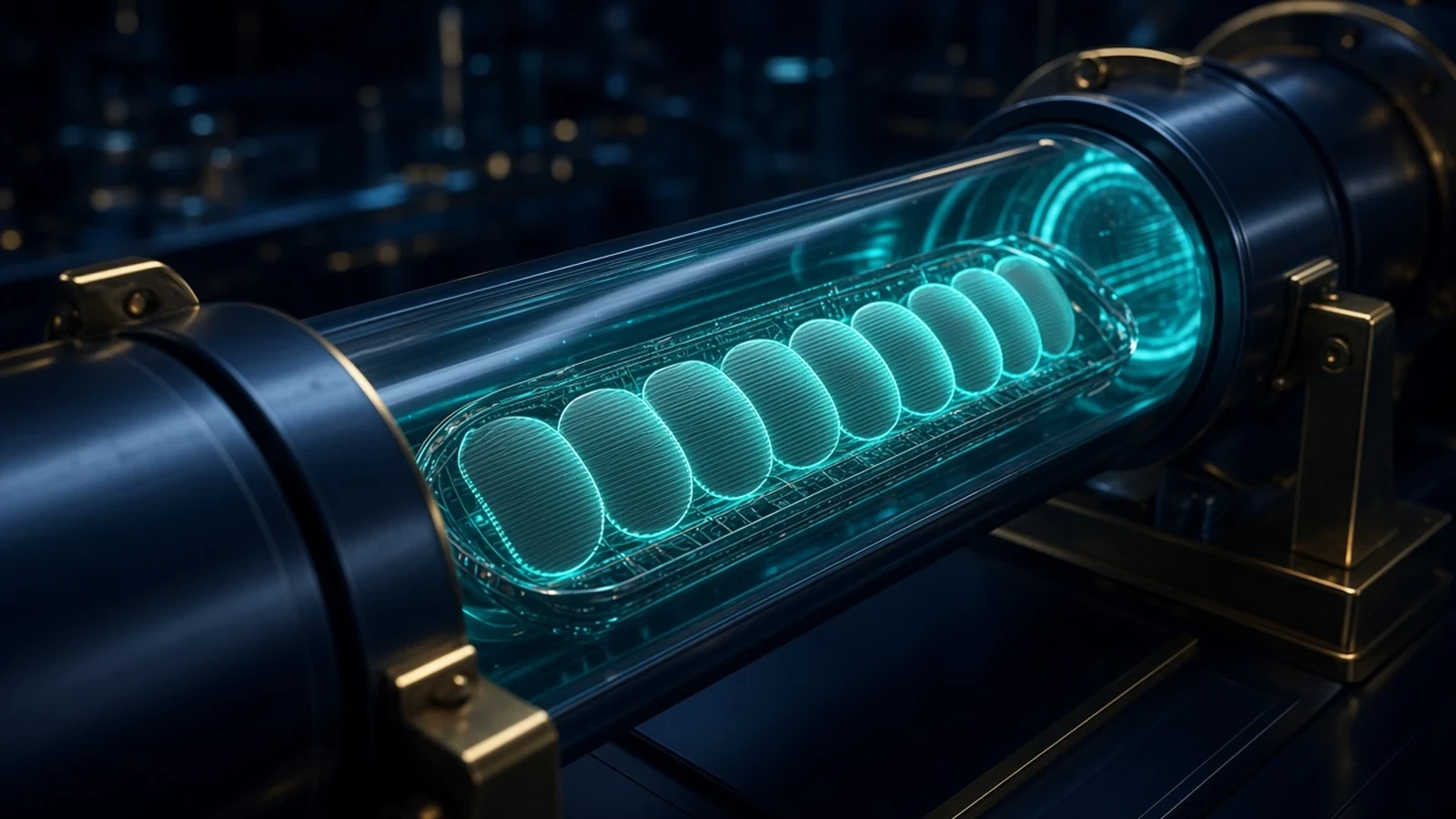
Kokusai Batch ALD combines atomic-layer deposition with multi-wafer batch furnaces for 3D device films.
AI & HPCData CenterConsumer ElectronicsView Technology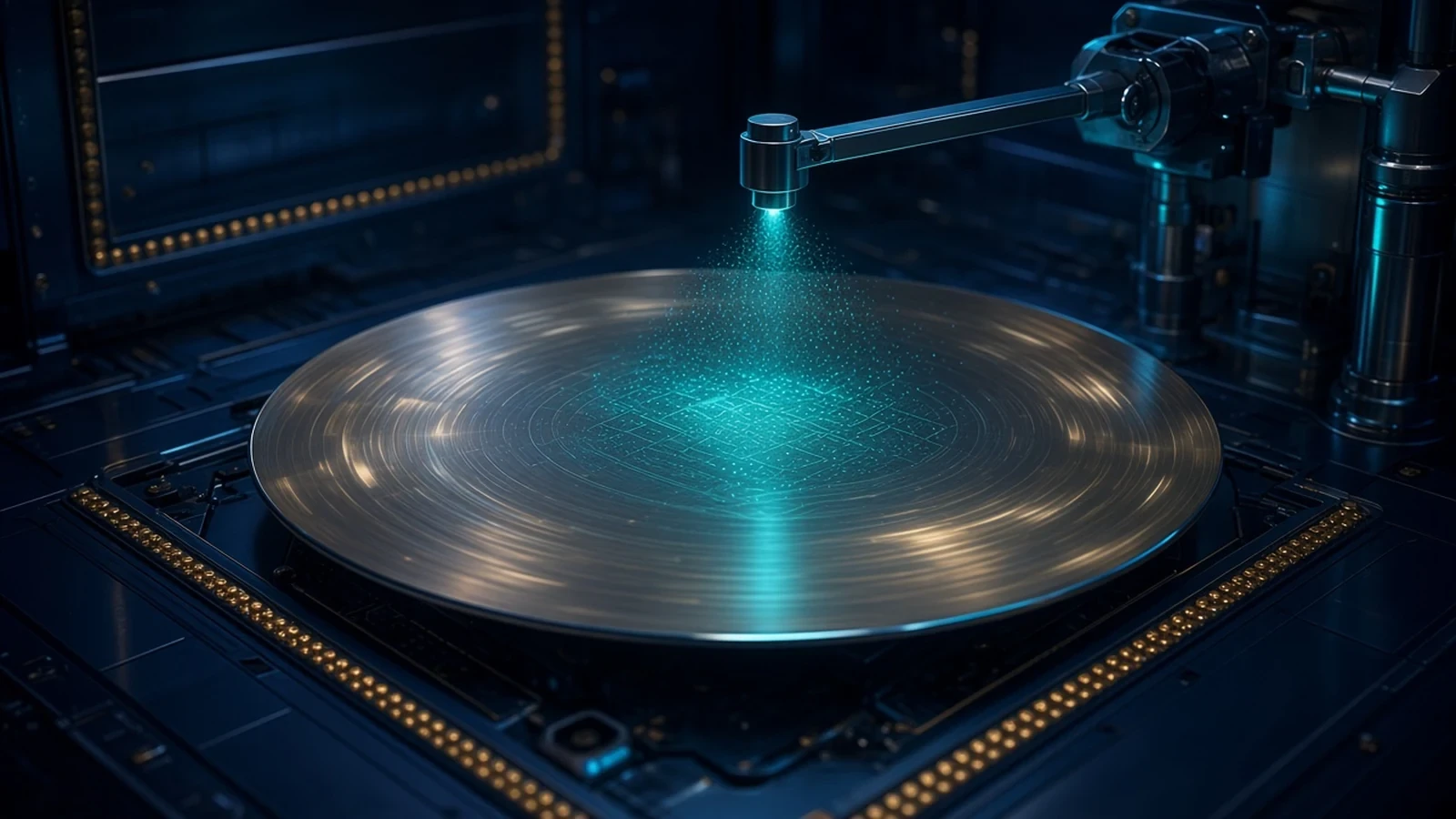
SCREEN SU Series is a single-wafer cleaning equipment family, currently described through SU-3400.
AutomotiveAI & HPCConsumer ElectronicsView Technology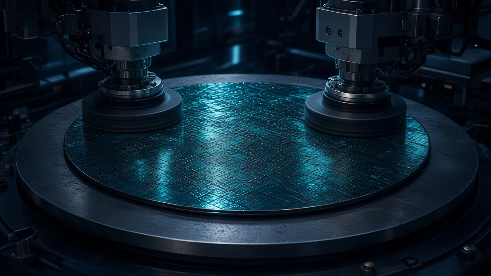
Hwatsing Universal-H300 is a 300 mm chemical-mechanical polishing tool for integrated circuits, advanced packaging and silicon wafers.
AutomotiveAI & HPCIndustrial+1View Technology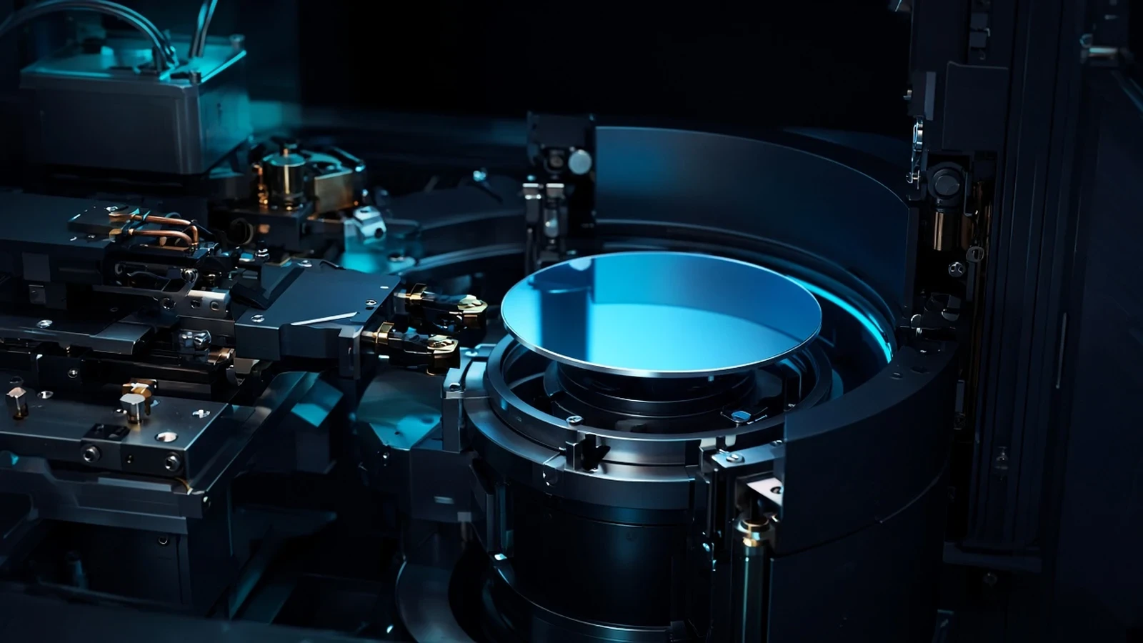
Tokyo Electron CLEAN TRACK LITHIUS is a coater/developer track platform used with lithography tools in high-volume wafer fabrication.
AutomotiveAI & HPCData Center+1View Technology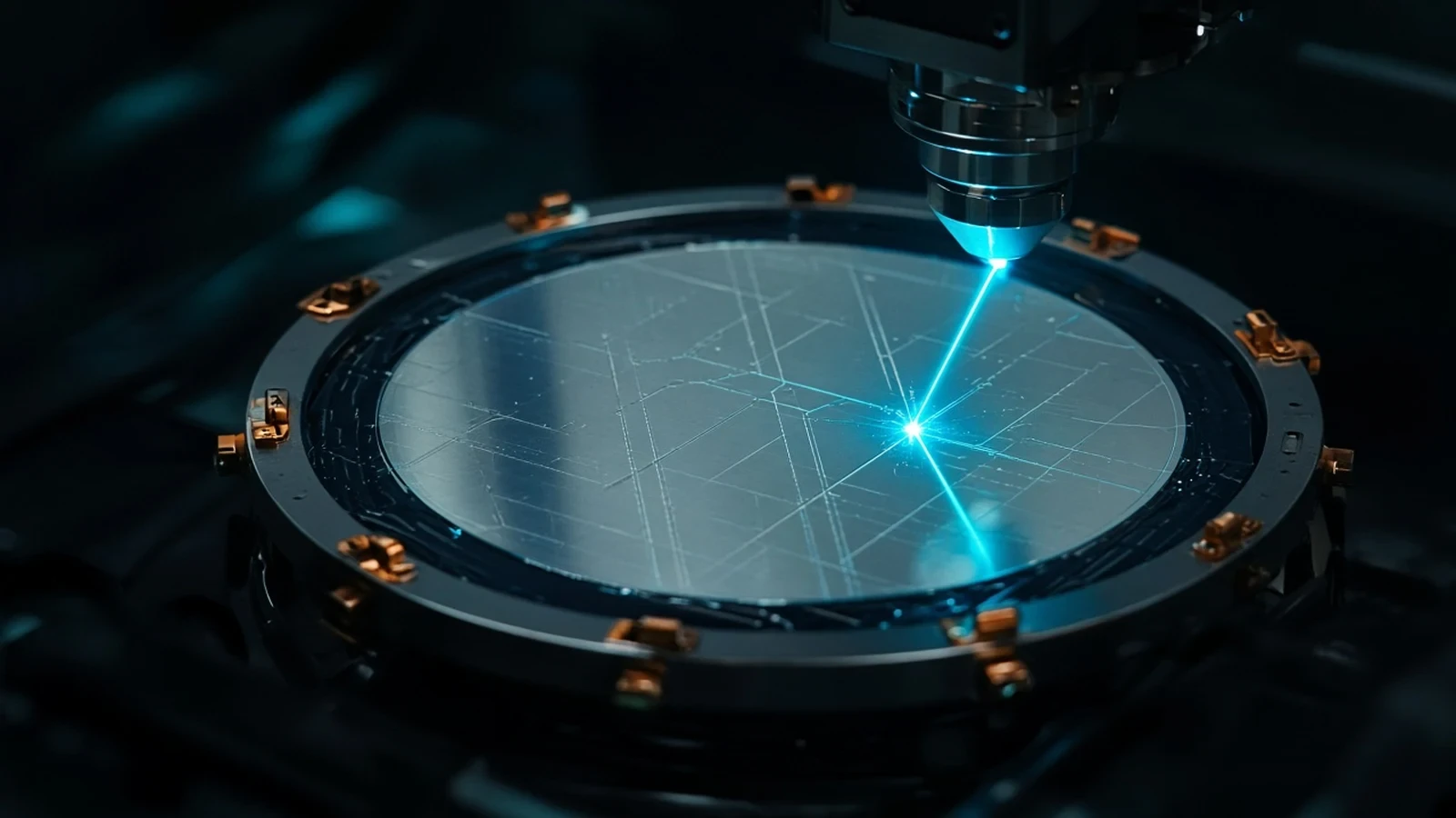
DISCO DBG with DAF laser cut is a dicing-before-grinding process that laser-cuts die-attach film during wafer thinning.
AutomotiveAI & HPCConsumer ElectronicsView Technology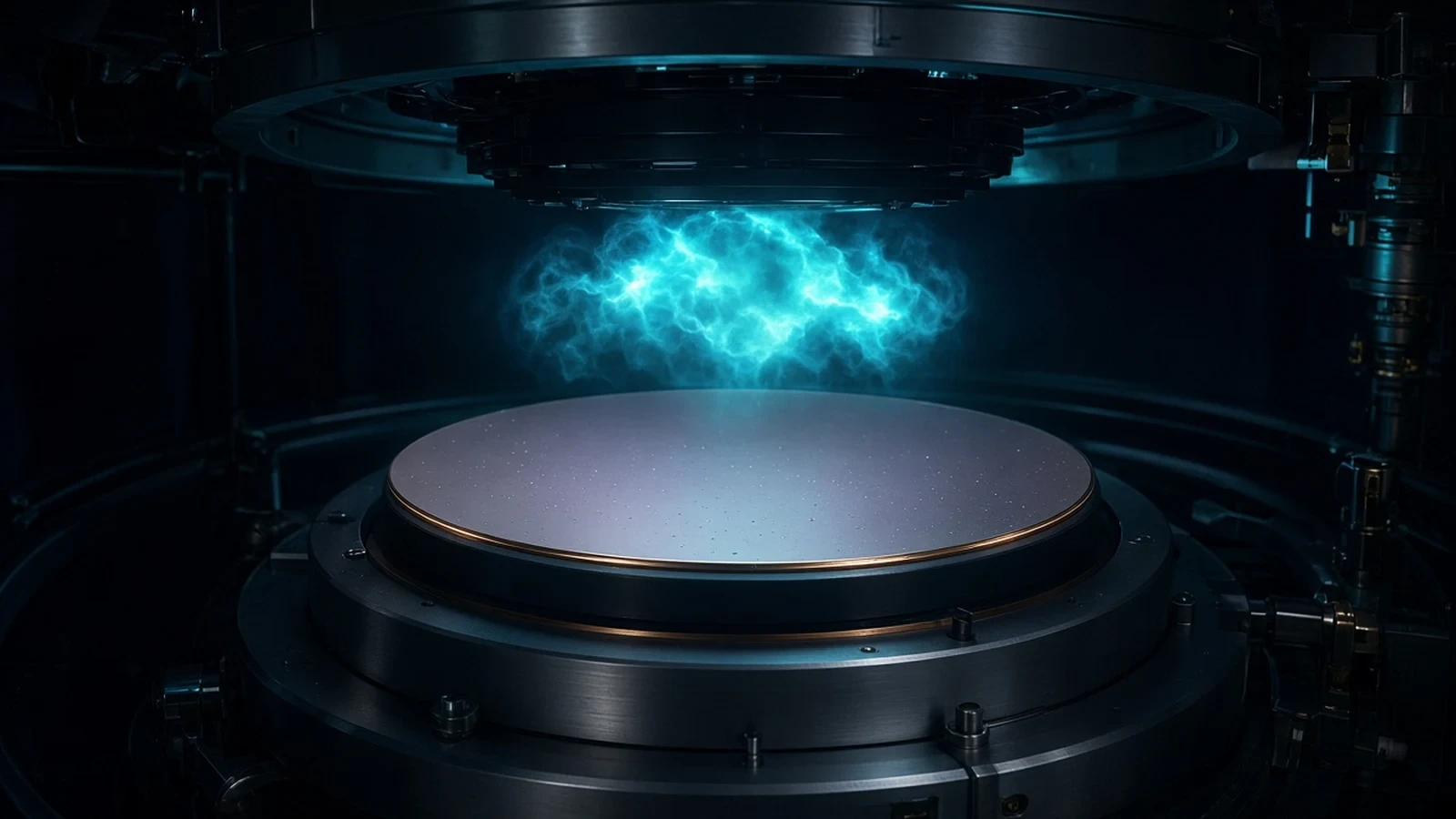
NAURA’s plasma etch platform is a wafer-fabrication etch tool family published on NAURA’s official product pages.
AutomotiveAI & HPCIndustrial+1View Technology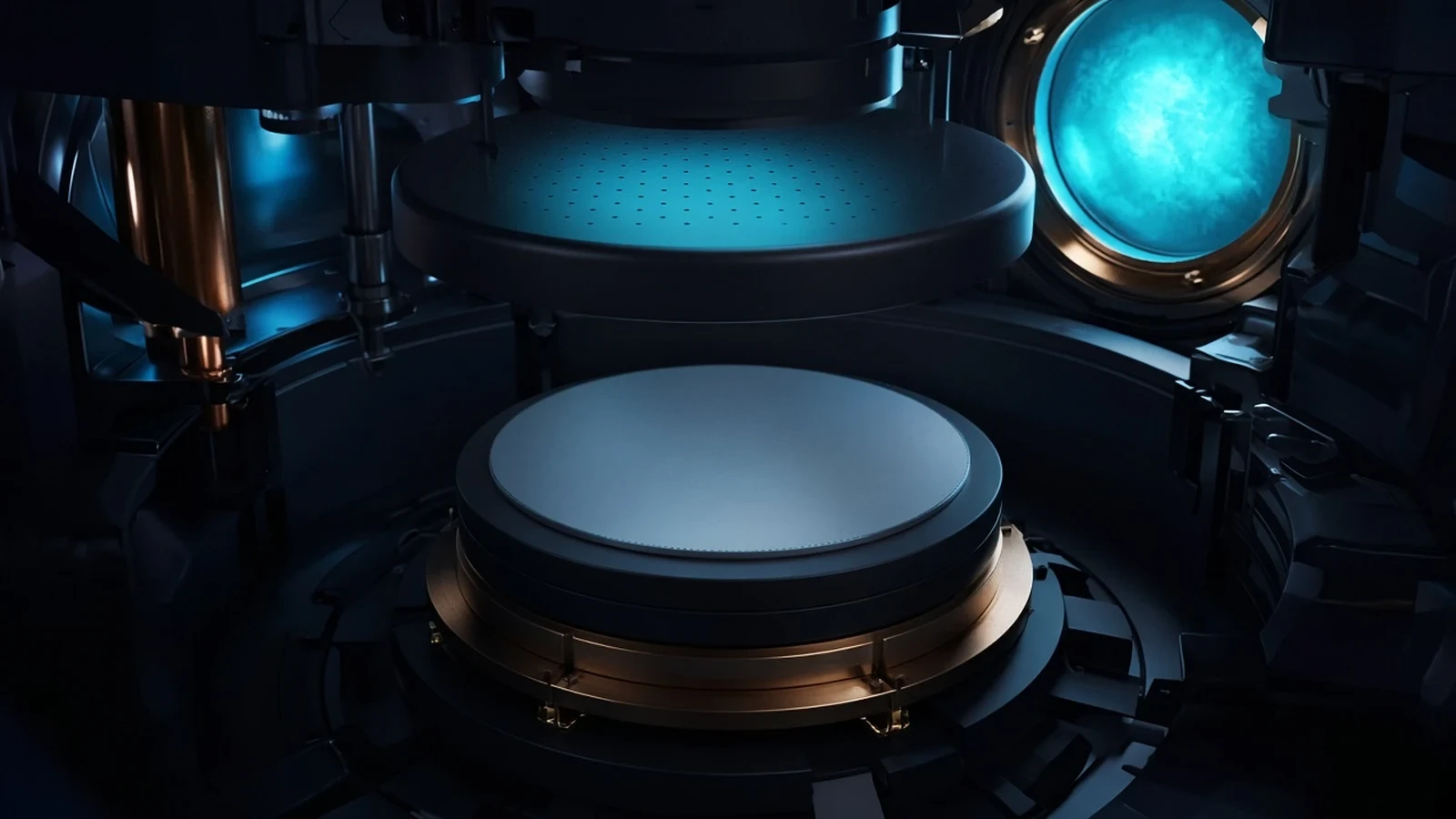
AMEC Primo is a plasma etch equipment platform published on AMEC’s official product pages.
AI & HPCData CenterConsumer ElectronicsView Technology
ASML TWINSCAN DUV is the deep-ultraviolet lithography platform covering immersion and dry scanners that print most chip layers alongside EUV. Distinct from NXE and High-NA EXE EUV.
AI & HPCConsumer ElectronicsView Technology
ASML TWINSCAN NXE is the 0.33 numerical-aperture EUV lithography platform used in high-volume manufacturing of advanced logic and memory chips. Distinct from High-NA EXE systems.
AI & HPCConsumer ElectronicsView Technology
ASM Atomic Layer Deposition technology enables highly controlled, layer-by-layer deposition of ultrathin conformal films for advanced semiconductor logic, memory and packaging structures.
AI & HPCData CenterConsumer ElectronicsView Technology
Lam Research wafer-process equipment category for thin-film deposition, plasma etch, strip, clean and related fabrication steps. SABRE ECD is listed separately.
Data CenterConsumer ElectronicsView Technology
ASML High-NA EUV lithography platform (TWINSCAN EXE) using 0.55 numerical aperture optics. Distinct from 0.33 NA TWINSCAN NXE EUV systems.
AI & HPCConsumer ElectronicsView Technology