Skip to content
Silicon Showcase
CompaniesApplicationsTechnology AreasAbout
Submit Technology
Submit Technology
Silicon Showcase

Silicon Showcase™ is the global directory of semiconductor technologies, platforms and innovations from around the world.

  • Technologies
  • Technology Signals
  • Companies
  • Applications
  • Technology Areas
  • About Us
  • How It Works
  • Submit Technology
  • Contact Us
  • Privacy Policy
  • Terms of Use
  • Disclaimer

Explore

  • Technologies
  • Technology Signals
  • Companies
  • Applications
  • Technology Areas

About

  • About Us
  • How It Works
  • Submit Technology
  • Contact Us

Legal

  • Privacy Policy
  • Terms of Use
  • Disclaimer

© 2026 Silicon Showcase™. All rights reserved.

Explore. Compare. Innovate.

Silicon Showcase
CompaniesApplicationsTechnology AreasAbout
Submit Technology
Submit Technology
Silicon Showcase

Silicon Showcase™ is the global directory of semiconductor technologies, platforms and innovations from around the world.

  • Technologies
  • Technology Signals
  • Companies
  • Applications
  • Technology Areas
  • About Us
  • How It Works
  • Submit Technology
  • Contact Us
  • Privacy Policy
  • Terms of Use
  • Disclaimer

Explore

  • Technologies
  • Technology Signals
  • Companies
  • Applications
  • Technology Areas

About

  • About Us
  • How It Works
  • Submit Technology
  • Contact Us

Legal

  • Privacy Policy
  • Terms of Use
  • Disclaimer

© 2026 Silicon Showcase™. All rights reserved.

Explore. Compare. Innovate.

  1. Home
  2. /Technologies
  3. /ERS Fully Automated 310 × 310 mm Panel-Level Packaging System

310 × 310

310 × 310 mm panel-level packaging platform
INTEGRATES TEMPORARY CARRIER

Integrates temporary carrier bonding, debonding and detaping

APPLICATIONS

AI & HPC · Data Center

Official technology image

310 × 310

310 × 310 mm panel-level packaging platform

INTEGRATES TEMPORARY CARRIER

Integrates temporary carrier bonding, debonding and detaping

APPLICATIONS

AI & HPC · Data Center

Public source

ERS Fully Automated 310 × 310 mm Panel-Level Packaging System

Manufacturing Equipment

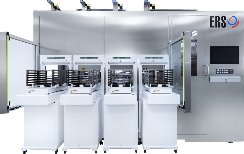
ERS electronic announced a fully automated panel-level packaging (PLP) system for 310 × 310 mm substrates on its official automated-PLP page.

  • AI & HPC
  • Data Center
GermanyView Official Source (opens in a new tab)

Official technology image

Overview

Fully automated 310 × 310 mm panel-level packaging system from ERS electronic that integrates temporary carrier bonding, debonding and detaping. The first unit has been delivered to a semiconductor manufacturer for panel-line integration.

The machine integrates temporary carrier bonding, debonding and detaping into one automated platform rated at 13 panels per hour, so panels move between process modules rather than between separate tools. ERS says that dual-carrier bonding and debonding workflows are increasingly important for backside processing in 3D IC, HBM and 2.5D IC packaging, and that the 310 × 310 mm panel format improves substrate-area utilisation compared with 300 mm circular wafers. The system is developed and manufactured at ERS’s Advanced Packaging facility in Barbing, Germany. The first unit has been delivered to a leading semiconductor manufacturer for integration into its panel production line. This listing records the announced system and first-unit delivery; it does not describe a broadly shipped product family beyond that statement.

Capabilities

Key characteristics associated with this technology.

  • 310 × 310 mm panel-level packaging platform

  • Integrates temporary carrier bonding, debonding and detaping

  • 13 panels per hour; in-tool module transfers instead of inter-tool moves

  • First unit delivered for integration into a manufacturer’s panel line

Organization

ERS electronic

Germany

View organization

Official resources

  • ERS electronic automated PLP systemers-gmbh.com (opens in a new tab)

Source & disclosure

Independent discovery listing. This profile was prepared from publicly available information published by the organization. For the latest and complete technical information, refer to the official company source.

Official source

ers-gmbh.com (opens in a new tab)

Last source check

Oct 3, 2026

Notice something that needs updating?

Report a correction

Related Technologies

Explore other semiconductor technologies.
Connectivity & RF

224G Linear Optical Connectivity Portfolio

Newly introduced Semtech 224G linear TIA and driver portfolio (GN1838L, GN42T380 and GN42M380) for near-packaged and co-packaged optics. Contact Semtech for availability.

AI & HPCData CenterView Technology
Materials & Substrates

300mm High-Thermal-Conductivity SiC Substrates

Coherent has begun customer sampling of 300 mm high-thermal-conductivity silicon carbide substrates intended as heat-spreading materials for AI and HPC infrastructure.

AI & HPCData CenterView Technology
Memory & Storage

512GB DDR5 RDIMM

Micron 512GB DDR5 RDIMM is the ultra-dense server module Micron demonstrated on 15 September 2026, with speeds up to 9,200 MT/s. Volume production is expected in the second half of 2027.

AI & HPCData CenterView Technology
Advanced Packaging

Embedded Power Platform (EPP)

onsemi Embedded Power Platform (EPP) is a newly introduced wafer-level power-device integration architecture that uses the silicon wafer as the package. Sampling is expected in 2026 with strategic customers.

AutomotiveAI & HPCView Technology