Technology Area
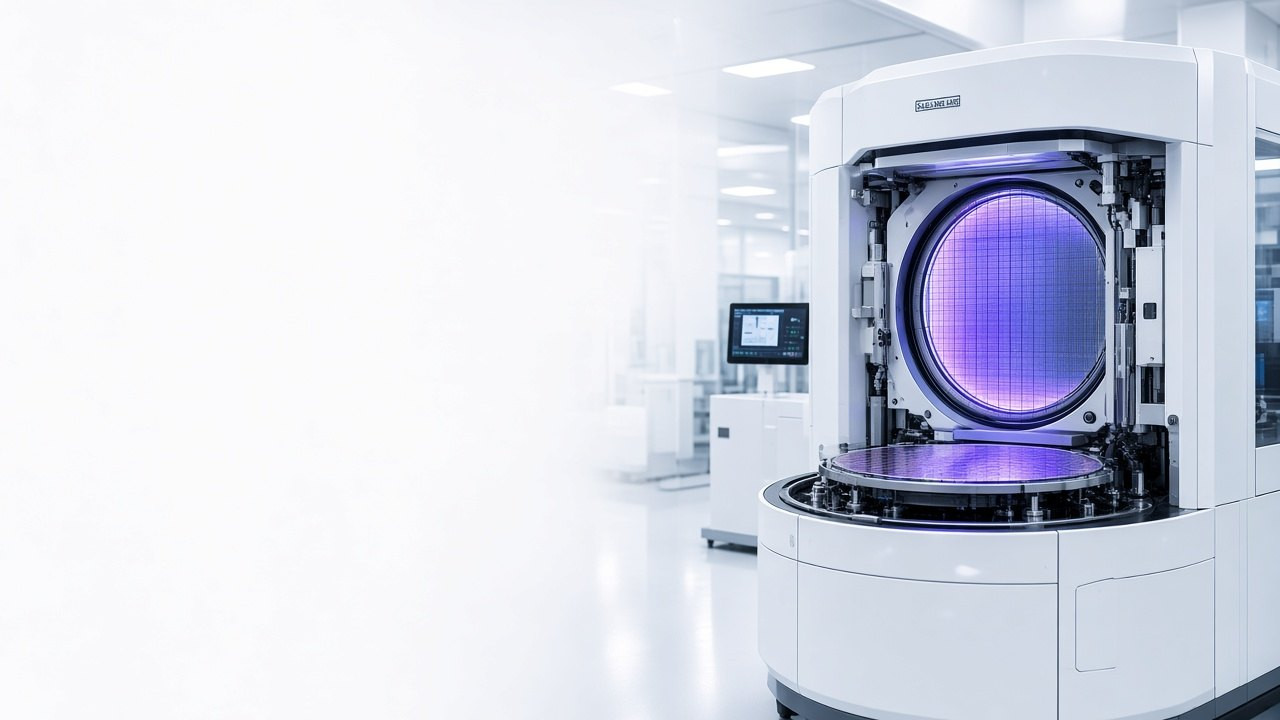
Lithography, deposition, etch and related process equipment used to fabricate semiconductors.
20
Technologies
15
Companies
7
Applications
Manufacturing equipment spans the full semiconductor fabrication process, including lithography, deposition, etch, inspection, metrology and various specialized tools. These systems enable the production of advanced logic, memory and compound semiconductor devices, supporting continued innovation across the industry.
Discover technologies, solutions and innovations in this area.

ASM Atomic Layer Deposition technology enables highly controlled, layer-by-layer deposition of ultrathin conformal films for advanced semiconductor logic, memory and packaging structures.
AI & HPCData CenterConsumer ElectronicsView Technology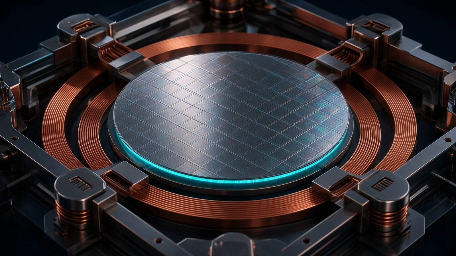
ASM epitaxy is a crystalline film-growth equipment platform covering silicon and silicon-germanium transistor epitaxy and silicon carbide epitaxy. Distinct from ASM atomic layer deposition.
AutomotiveAI & HPCEnergyView Technology
ASML TWINSCAN DUV is the deep-ultraviolet lithography platform covering immersion and dry scanners that print most chip layers alongside EUV. Distinct from NXE and High-NA EXE EUV.
AI & HPCConsumer ElectronicsView TechnologyKey application areas leveraging these technologies.
Technology area visuals are illustrative representations.