WAFER-LEVEL ARCHITECTURE THAT
Wafer-level architecture that uses the silicon wafer as the package
Wafer-level architecture that uses the silicon wafer as the package
Embeds FETs, drivers and controllers; RDLs replace wire bonds
Automotive · AI & HPC · Industrial · +1
Public source
Embedded Power Platform (EPP) is the power-device integration and packaging architecture published on onsemi’s official technology page and introduced on 16 September 2026.
Silicon Showcase illustrative visual
Illustrative representation based on publicly available technical information.
onsemi Embedded Power Platform (EPP) is a newly introduced wafer-level power-device integration architecture that uses the silicon wafer as the package. Sampling is expected in 2026 with strategic customers.
Unlike traditional power modules, EPP embeds multiple semiconductor die in a silicon wafer-level architecture and replaces wire bonds with wafer-level redistribution layers (RDLs). onsemi says the platform brings power, control and isolation functions together, and supports current and future generations of silicon, silicon carbide (SiC), gallium nitride (GaN) and emerging power technologies. The technology page states that co-optimized design delivers up to 4× improved power density. onsemi’s introduction also describes using the silicon wafer itself as the foundation of the package, 12-inch wafer manufacturing, and application figures that include 3–5× higher power density depending on the application; an early EPP-based solid-state circuit-breaker design described as about 50% smaller and 20% cooler; and traction-inverter figures of up to 4× higher power density and 15% lower power losses versus conventional approaches. Published application areas on the technology page are AI infrastructure, electric vehicles, charging infrastructure, renewable energy and industrial automation. Subaru is named as an early engagement partner evaluating the platform for future electrified vehicles. Availability: EPP is expected to begin sampling in 2026 with strategic customers and ecosystem participants across automotive and AI applications. This listing does not describe EPP as a generally available production catalog.
Key characteristics associated with this technology.
Wafer-level architecture that uses the silicon wafer as the package
Embeds FETs, drivers and controllers; RDLs replace wire bonds
Supports silicon, SiC, GaN and emerging power technologies
Up to 4× improved power density on onsemi’s technology page; sampling expected in 2026
Explore other semiconductor technologies.
Newly introduced Semtech 224G linear TIA and driver portfolio (GN1838L, GN42T380 and GN42M380) for near-packaged and co-packaged optics. Contact Semtech for availability.
AI & HPCData CenterView Technology
Coherent has begun customer sampling of 300 mm high-thermal-conductivity silicon carbide substrates intended as heat-spreading materials for AI and HPC infrastructure.
AI & HPCData CenterView Technology
Micron 512GB DDR5 RDIMM is the ultra-dense server module Micron demonstrated on 15 September 2026, with speeds up to 9,200 MT/s. Volume production is expected in the second half of 2027.
AI & HPCData CenterView Technology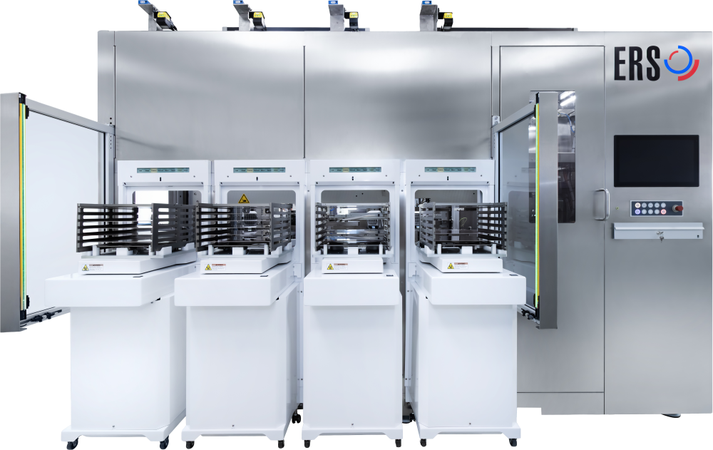
Fully automated 310 × 310 mm panel-level packaging system from ERS electronic that integrates temporary carrier bonding, debonding and detaping. The first unit has been delivered to a semiconductor manufacturer for panel-line integration.
AI & HPCData CenterView Technology