Discover 169 technologies from leading innovators around the world.
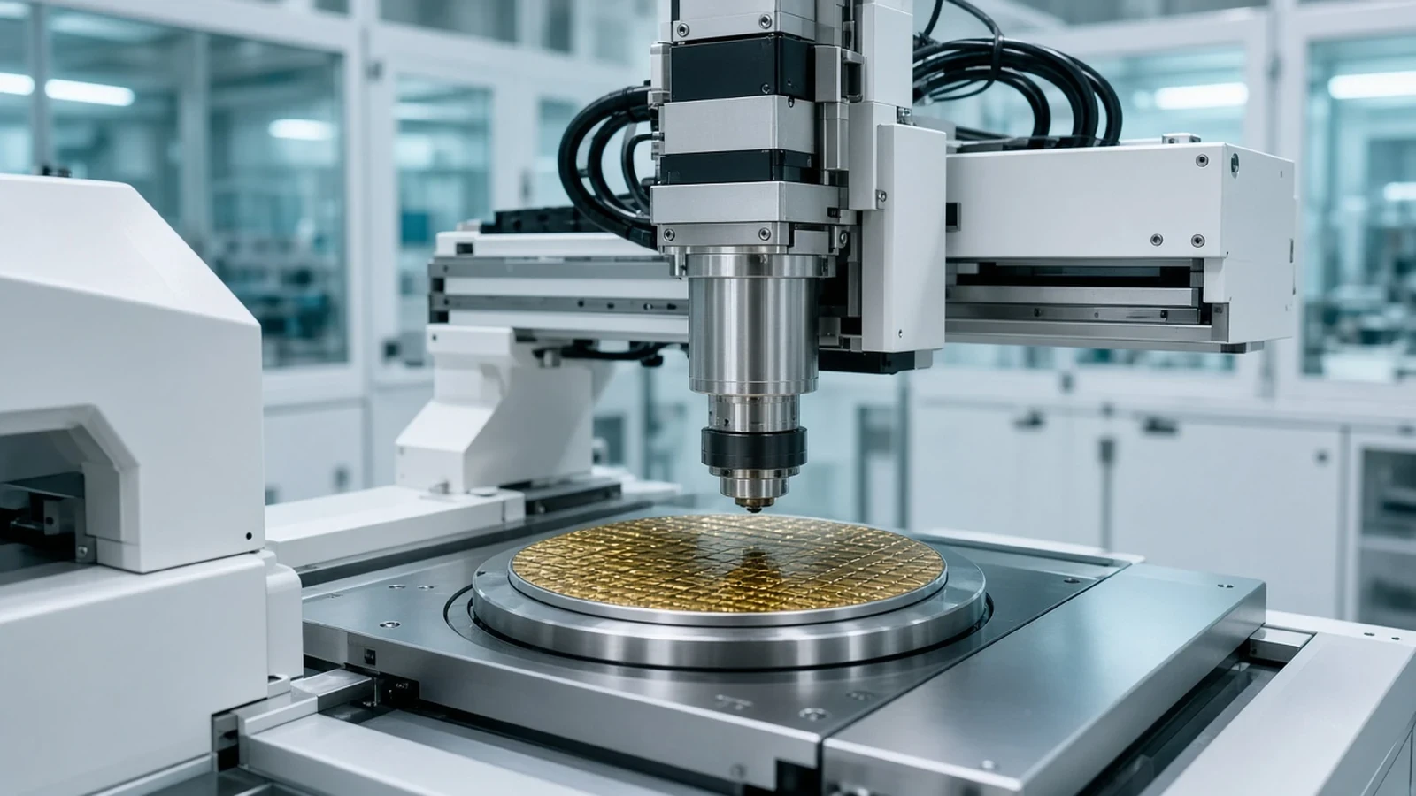
Kulicke & Soffa APTURA is a thermo-compression bonder for advanced packaging, not a wire bonder catalog and not OSAT assembly.
AI & HPCData Center+1View Technology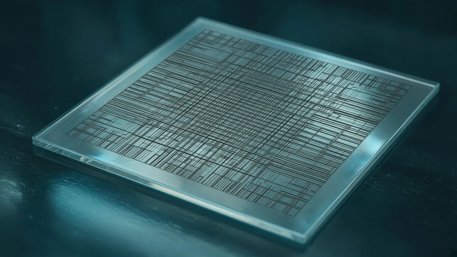
Photronics advanced IC photomasks are lithography reticles for integrated circuits, not a foundry node and not FPD masks.
AutomotiveAI & HPC+1View Technology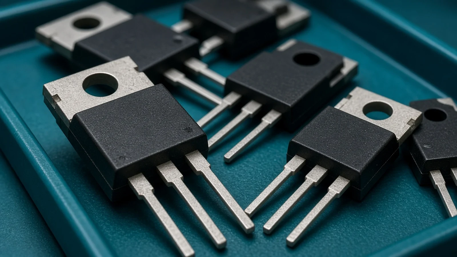
AlphaSGT is Alpha and Omega’s shielded-gate trench MOSFET technology, not a GaN HEMT and not a power-module substrate.
AI & HPCData Center+1View Technology
QuickLogic Australis is embedded FPGA IP, not a standalone FPGA chip and not a foundry process.
AI & HPCIndustrial+2View Technology
CEVA-NeuPro-Nano is edge NPU processor IP, not a discrete accelerator chip and not a full SoC.
AI & HPCConsumer Electronics+1View Technology
Cohu Diamondx is semiconductor ATE instrumentation, not a handler and not a probe card.
AutomotiveAI & HPC+2View Technology
Aehr FOX-XP is a multi-wafer burn-in and test system, not a packaged-device ATE rack and not a probe card.
AutomotiveAI & HPC+1View Technology
Arteris FlexNoC is on-chip network IP, not a packaged interconnect chip and not a coherent cache controller.
AutomotiveAI & HPC+1View Technology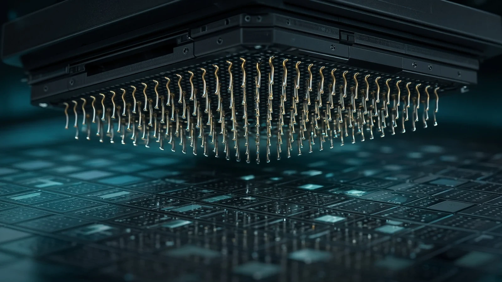
Micronics Japan MEMS-SP is a MEMS probe-card technology for wafer test, not a handler and not a packaged-device socket.
AutomotiveAI & HPC+1View Technology
Ambiq SPOT is subthreshold MCU circuit technology, not a wireless protocol stack and not a foundry process.
AI & HPCConsumer Electronics+2View Technology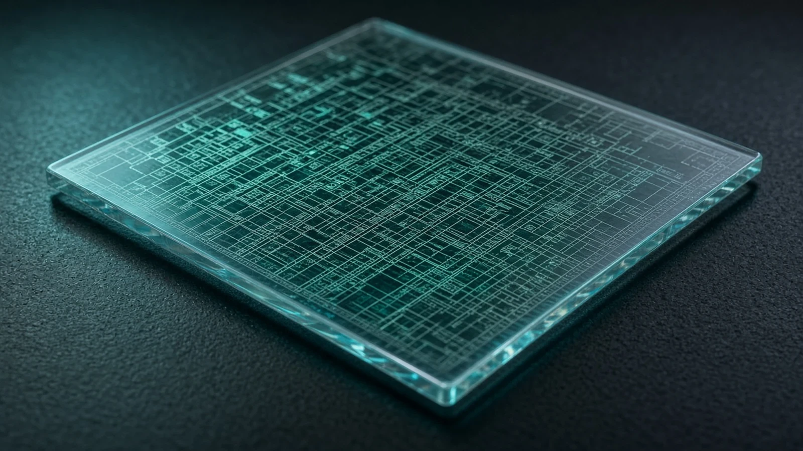
Tekscend semiconductor photomasks are lithography reticles, not a foundry process node and not a mask writer.
AutomotiveAI & HPC+1View Technology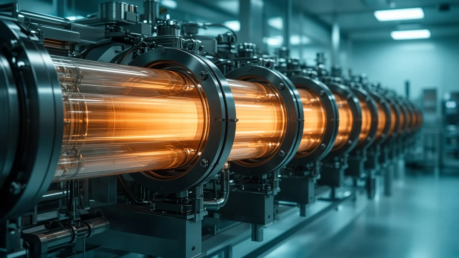
centrotherm c.HORICOO 300 is a 300 mm horizontal furnace platform, not a deposition-materials consumable.
AutomotiveAI & HPC+1View Technology
GUC APT is a 2.5D/3D multi-die ASIC packaging-design platform, not a foundry process node and not OSAT assembly.
AI & HPCData Center+1View Technology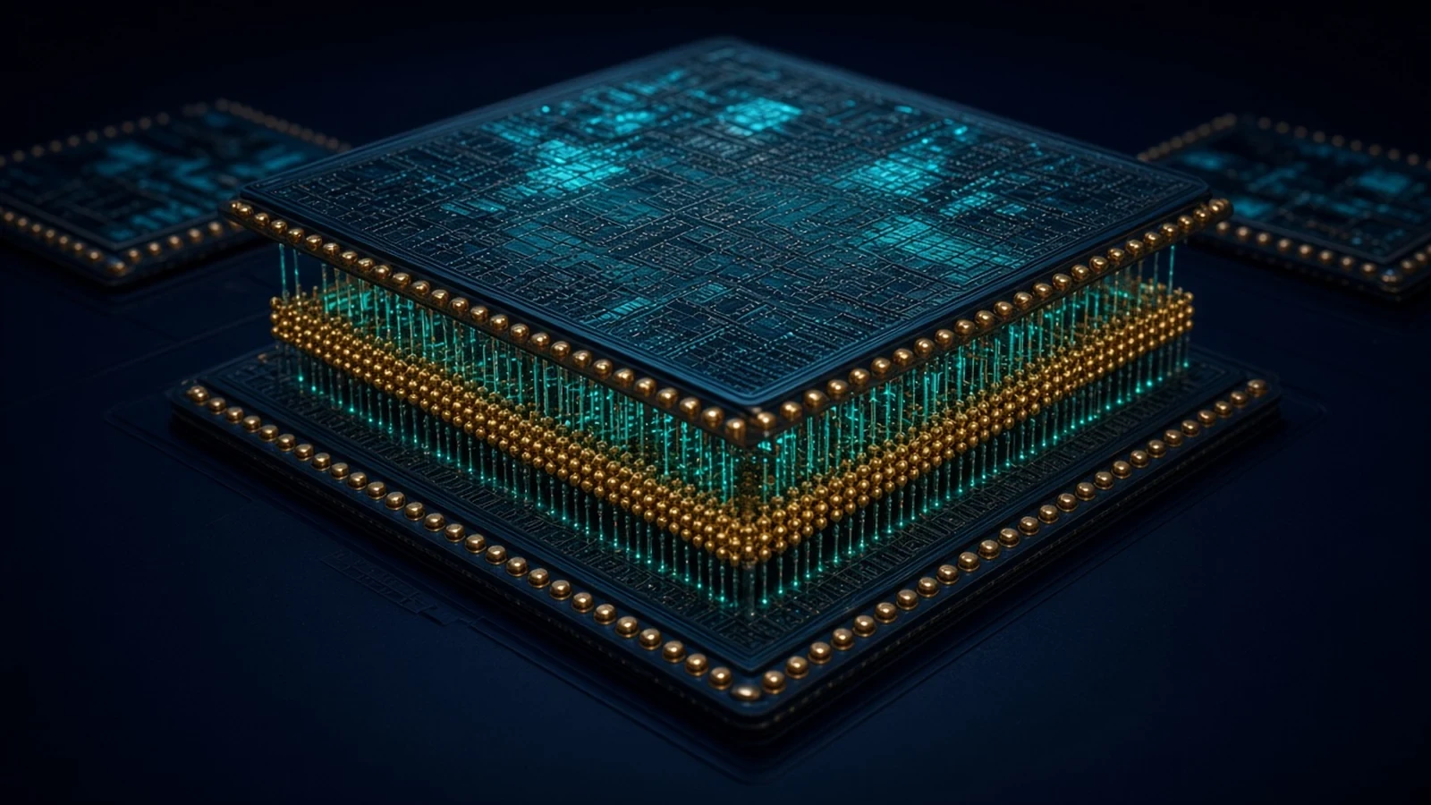
Powerchip 3D AI Foundry is a wafer-on-wafer logic/memory stacking foundry offering, parked in Advanced Packaging because Foundry / Process does not yet exist.
AutomotiveAI & HPC+1View Technology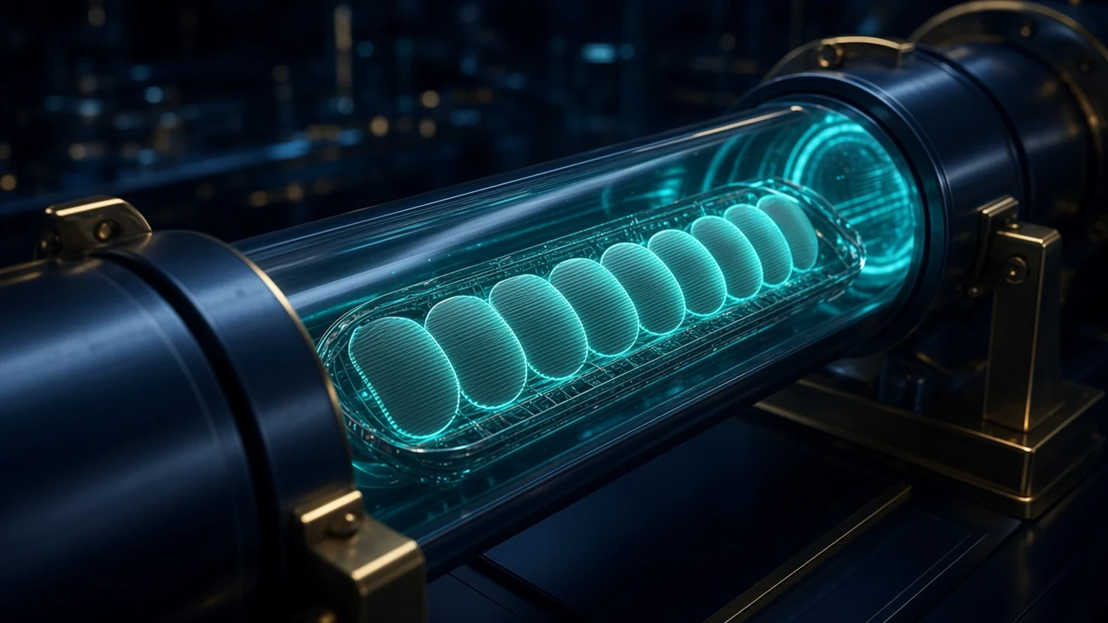
Kokusai Batch ALD combines atomic-layer deposition with multi-wafer batch furnaces for 3D device films.
AI & HPCData Center+1View Technology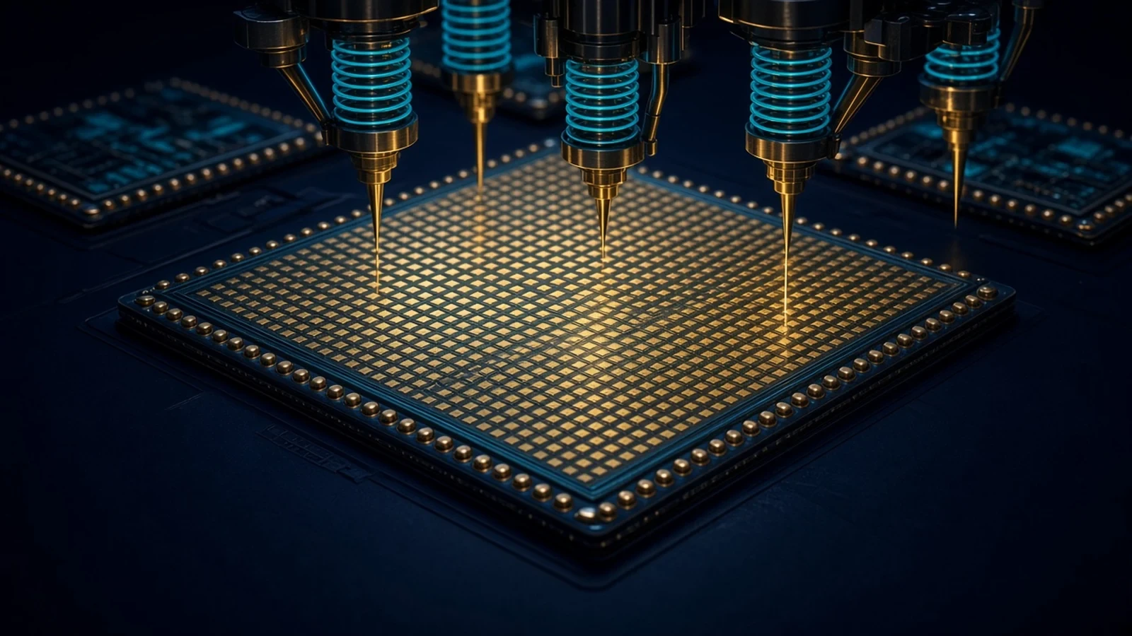
FormFactor composite-metal MEMS is a wafer-probe-card technology, not a MEMS sensor product.
AutomotiveAI & HPC+1View Technology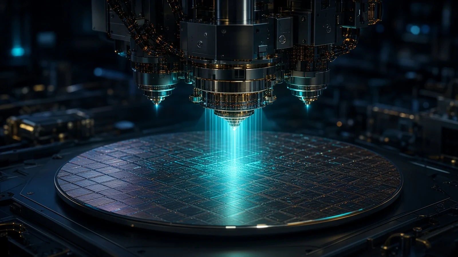
Camtek Eagle is a wafer inspection and metrology equipment platform for BEOL, advanced packaging and related flows.
AutomotiveAI & HPC+1View Technology
Qnity Emblem is a next-generation CMP pad platform for advanced-node planarization, not a polishing tool.
AI & HPCData Center+1View Technology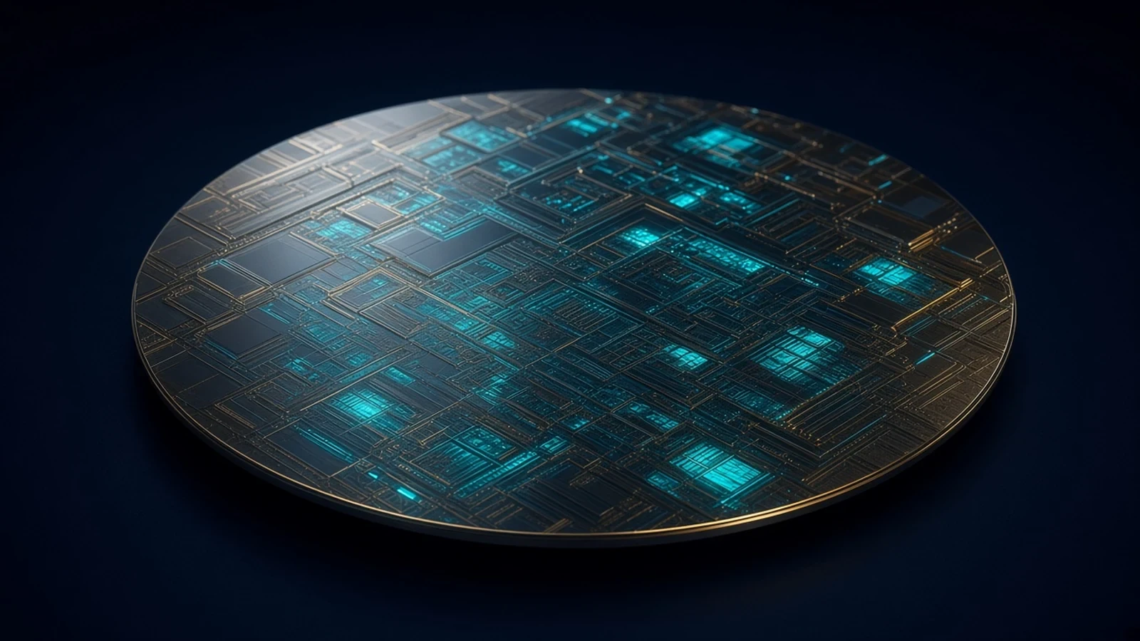
GlobalWafers Silicon Wafers are the company's silicon starting substrates, including annealed, epitaxial, SOI and diffusion wafers.
AutomotiveAI & HPC+2View Technology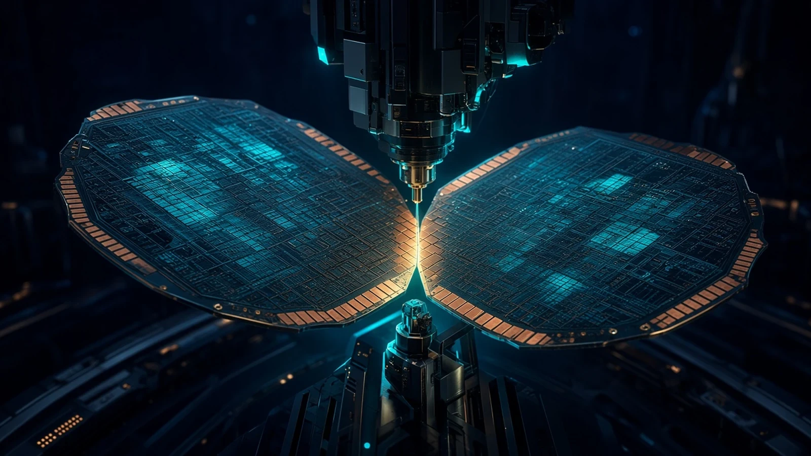
ASMPT LITHOBOLT G2 is a die-to-wafer hybrid-bonding system for direct and collective bonding.
AutomotiveAI & HPC+1View Technology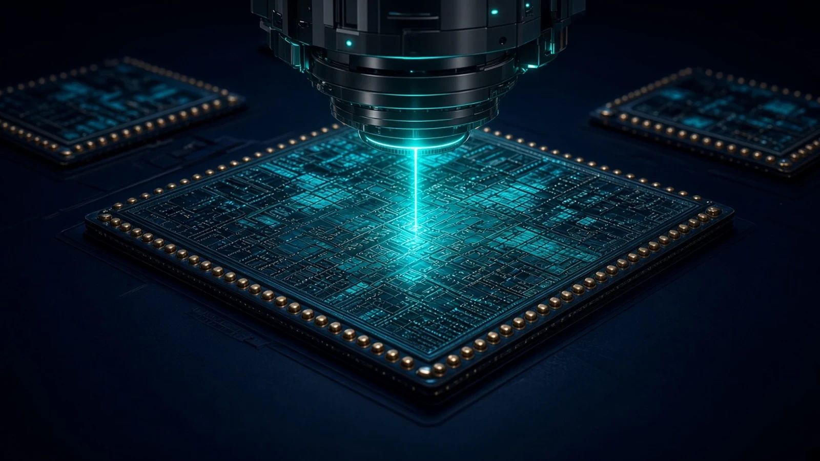
Nova’s multidisciplinary metrology platform combines optical scatterometry, X-ray and materials analysis for process control.
AutomotiveAI & HPC+1View Technology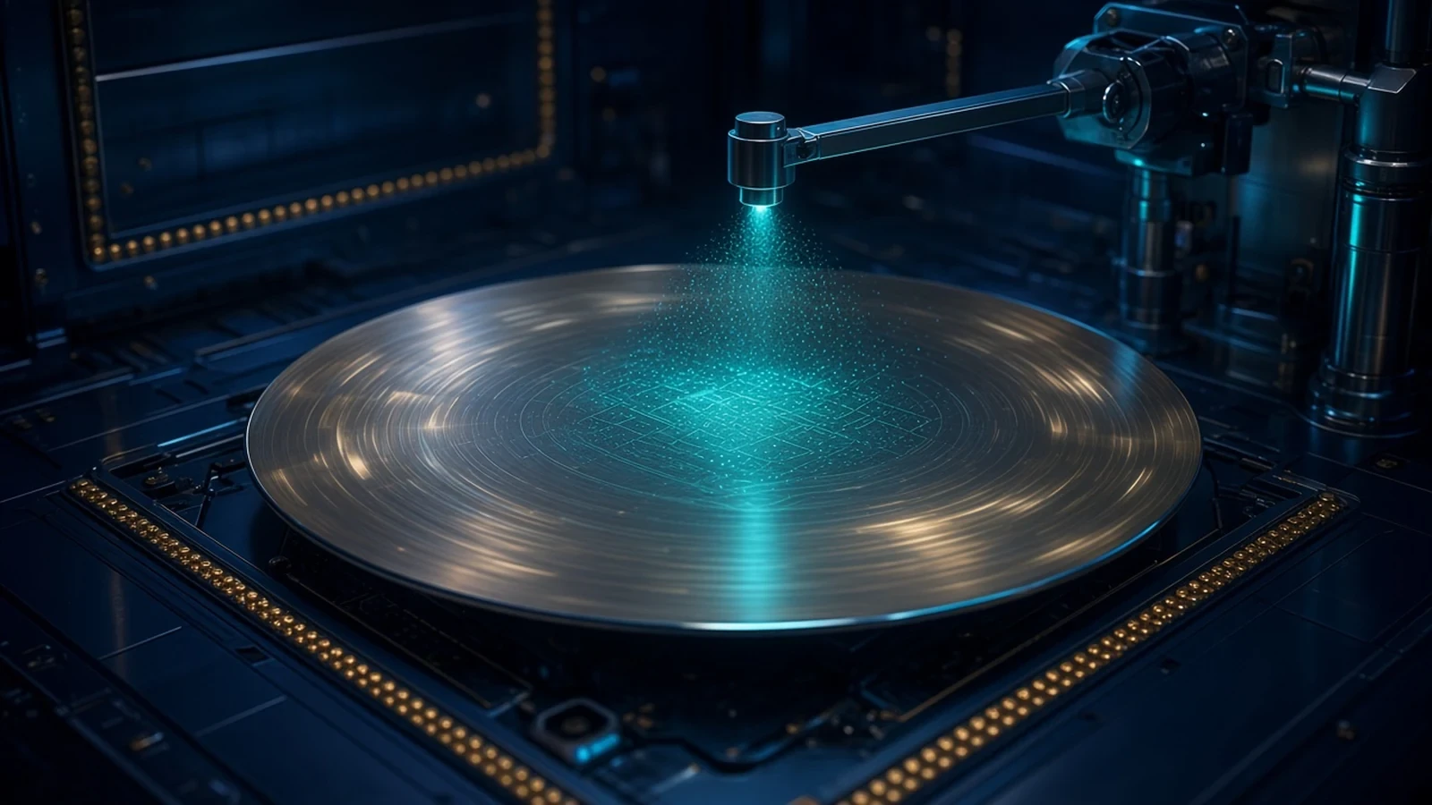
SCREEN SU Series is a single-wafer cleaning equipment family, currently described through SU-3400.
AutomotiveAI & HPC+1View Technology
SUMCO Advanced Silicon Wafers are polished and specialty silicon starting substrates, including epitaxial, annealed and SOI wafers.
AutomotiveAI & HPC+2View Technology
VeriSilicon SiPaaS is a platform-based custom-silicon design and turnkey service, not a foundry process node.
AutomotiveAI & HPC+2View Technology