Discover 169 technologies from leading innovators around the world.
Photronics advanced IC photomasks are lithography reticles for integrated circuits, not a foundry node and not FPD masks.
AlphaSGT is Alpha and Omega’s shielded-gate trench MOSFET technology, not a GaN HEMT and not a power-module substrate.
QuickLogic Australis is embedded FPGA IP, not a standalone FPGA chip and not a foundry process.
CEVA-NeuPro-Nano is edge NPU processor IP, not a discrete accelerator chip and not a full SoC.
Cohu Diamondx is semiconductor ATE instrumentation, not a handler and not a probe card.
Aehr FOX-XP is a multi-wafer burn-in and test system, not a packaged-device ATE rack and not a probe card.
Arteris FlexNoC is on-chip network IP, not a packaged interconnect chip and not a coherent cache controller.
Ambiq SPOT is subthreshold MCU circuit technology, not a wireless protocol stack and not a foundry process.
FormFactor composite-metal MEMS is a wafer-probe-card technology, not a MEMS sensor product.
Qnity Emblem is a next-generation CMP pad platform for advanced-node planarization, not a polishing tool.
ACM Ultra C is a wet-clean and wet-process equipment family, not an IR homepage listing.
The Dragonfly G5 System is Onto Innovation's advanced-packaging inspection and metrology system.
Entegris Advanced Deposition Materials is a process-materials platform for precursor and deposition chemistries used in semiconductor manufacturing.
Credo SerDes is high-speed serializer/deserializer silicon and IP for data-center and AI interconnect, not a compute accelerator architecture.
Astera Labs Intelligent Connectivity Platform is PCIe, CXL and Ethernet connectivity silicon for AI and data-center racks, not a compute accelerator architecture.
Amkor SWIFT is a high-density fan-out packaging platform for fine-pitch RDL and multi-die construction.
Cerebras Wafer-Scale Engine 3 is a wafer-scale AI processor: one chip occupying an entire 300mm wafer for large-model training and inference.
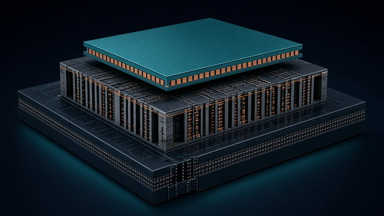
3D V-Cache stacks an L3 cache tile on a CPU core-complex die using copper-to-copper hybrid bonding and TSVs. Official AMD materials call it the first x86 true 3D die stack, with much higher interconnect density versus 2D chiplets.
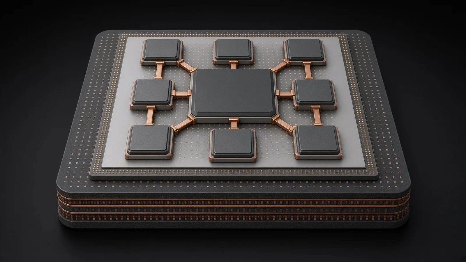
Infinity Fabric is AMD’s coherent on-package and multi-die interconnect, linking CPU core-complex dies to a central I/O die and, in multi-socket systems, across packages. Official EPYC architecture documents describe CCD–IOD GMI links and xGMI.
Trainium is AWS’s custom machine-learning training silicon, built around NeuronCore and used in EC2 Trn instances. Official AWS silicon pages describe purpose-built ML chips as part of AWS custom silicon.
Apple Silicon is Apple’s fabless SoC platform. The M1 newsroom introduction defines a system-on-chip with CPU, GPU, Neural Engine, I/O and unified memory on a single package so those engines share one memory pool.
Azure Maia 100 is Microsoft's first in-house cloud AI accelerator: 105 billion transistors on 5 nm, for Azure training and inference.
Broadcom’s CPO platform heterogeneously integrates optical engines (TSMC COUPE) with Ethernet switch silicon. Tomahawk 6–Davisson is the third-generation CPO switch: 102.4 Tbps optically enabled capacity and a claimed reduction in optical-interconnect power versus pluggables.
Tomahawk is Broadcom’s Ethernet switch-ASIC family for data-center and AI fabrics. Tomahawk 6 is the current generation: 102.4 Tbps in a single chip, 100G/200G SerDes, and an optional co-packaged optics variant.