Discover 169 technologies from leading innovators around the world.
Photronics advanced IC photomasks are lithography reticles for integrated circuits, not a foundry node and not FPD masks.
AutomotiveAI & HPC+1View Technology
CEVA-NeuPro-Nano is edge NPU processor IP, not a discrete accelerator chip and not a full SoC.
AI & HPCConsumer Electronics+1View Technology
Ambiq SPOT is subthreshold MCU circuit technology, not a wireless protocol stack and not a foundry process.
AI & HPCConsumer Electronics+2View Technology
Qnity Emblem is a next-generation CMP pad platform for advanced-node planarization, not a polishing tool.
AI & HPCData Center+1View Technology
Cirrus Halo Core is the DSP inside Cirrus haptic drivers, parked in Design & IP because Analog / Mixed Signal does not yet exist.
AutomotiveConsumer ElectronicsView Technology
Silicon Labs Series 3 is a next-generation wireless SoC platform, with SiXG302 sampling described as 2026.
IndustrialConsumer Electronics+2View Technology
Skyworks Sky5 is a 5G RF front-end system platform, not a foundry process and not a baseband SoC.
AutomotiveConsumer Electronics+2View Technology
TrenchFET Gen V Power MOSFETs are Vishay's current published trench power-MOSFET generation.
AutomotiveIndustrial+2View Technology
Texas Instruments analog BCD (LBC) is TI’s bipolar-CMOS-DMOS process identity for foundational analog and power silicon, described in official TI manufacturing communications.
AutomotiveIndustrial+2View Technology
Lattice Nexus is a low-power FPGA platform architecture, not a data-center compute accelerator architecture.
AutomotiveIndustrial+2View Technology
Amkor SWIFT is a high-density fan-out packaging platform for fine-pitch RDL and multi-die construction.
AI & HPCData Center+2View Technology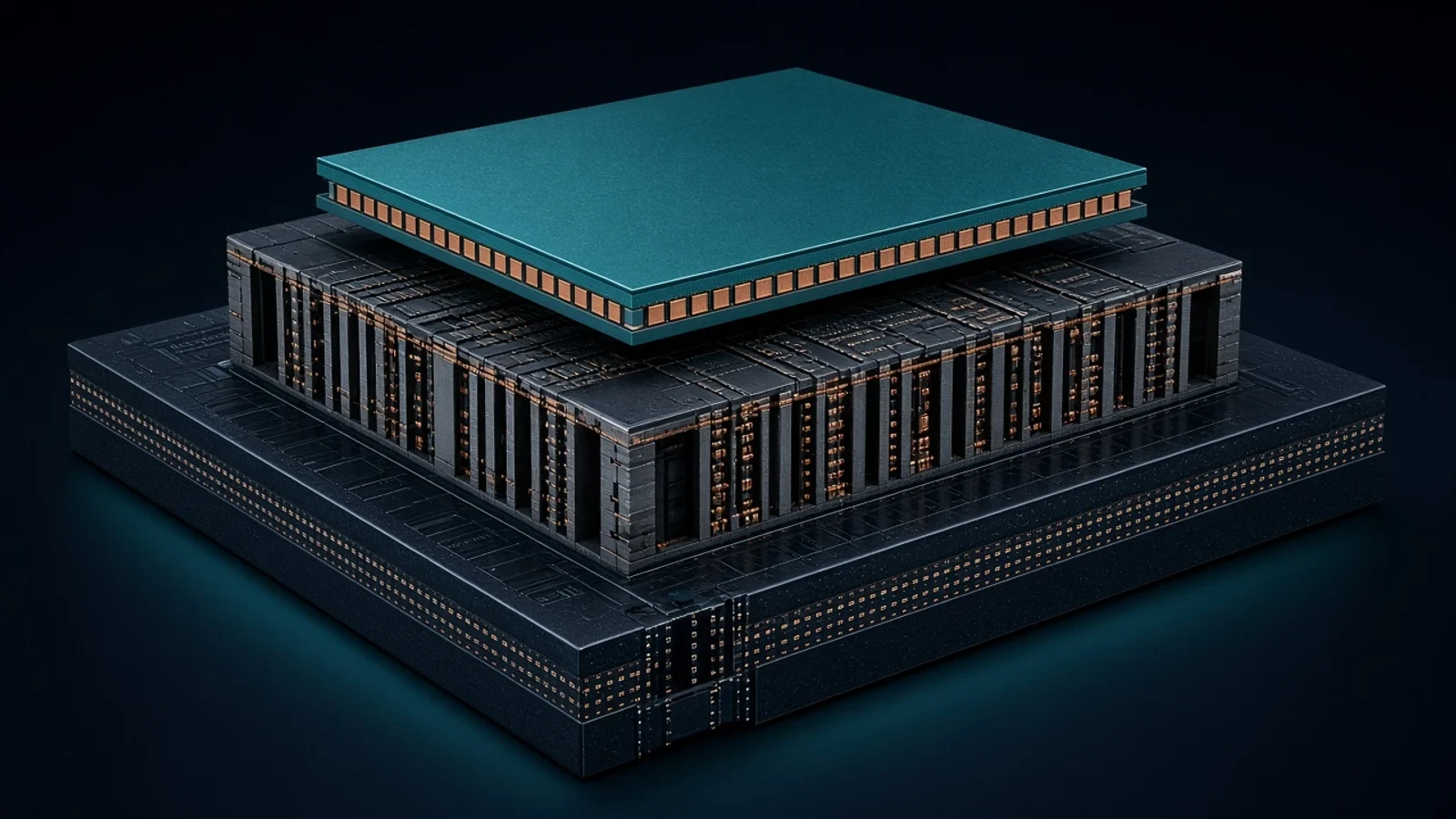
3D V-Cache stacks an L3 cache tile on a CPU core-complex die using copper-to-copper hybrid bonding and TSVs. Official AMD materials call it the first x86 true 3D die stack, with much higher interconnect density versus 2D chiplets.
AI & HPCData Center+1View Technology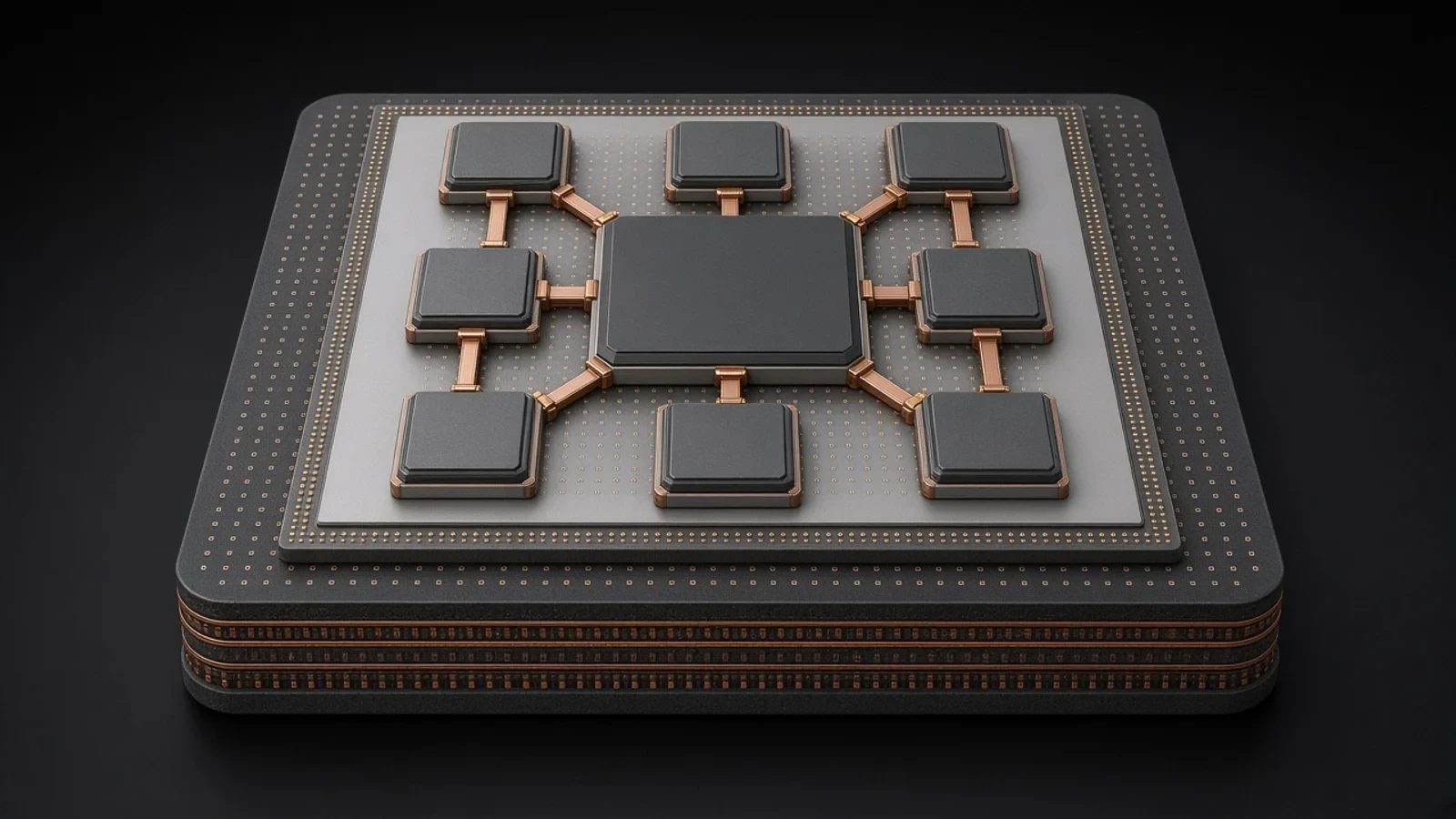
Infinity Fabric is AMD’s coherent on-package and multi-die interconnect, linking CPU core-complex dies to a central I/O die and, in multi-socket systems, across packages. Official EPYC architecture documents describe CCD–IOD GMI links and xGMI.
AI & HPCData Center+1View Technology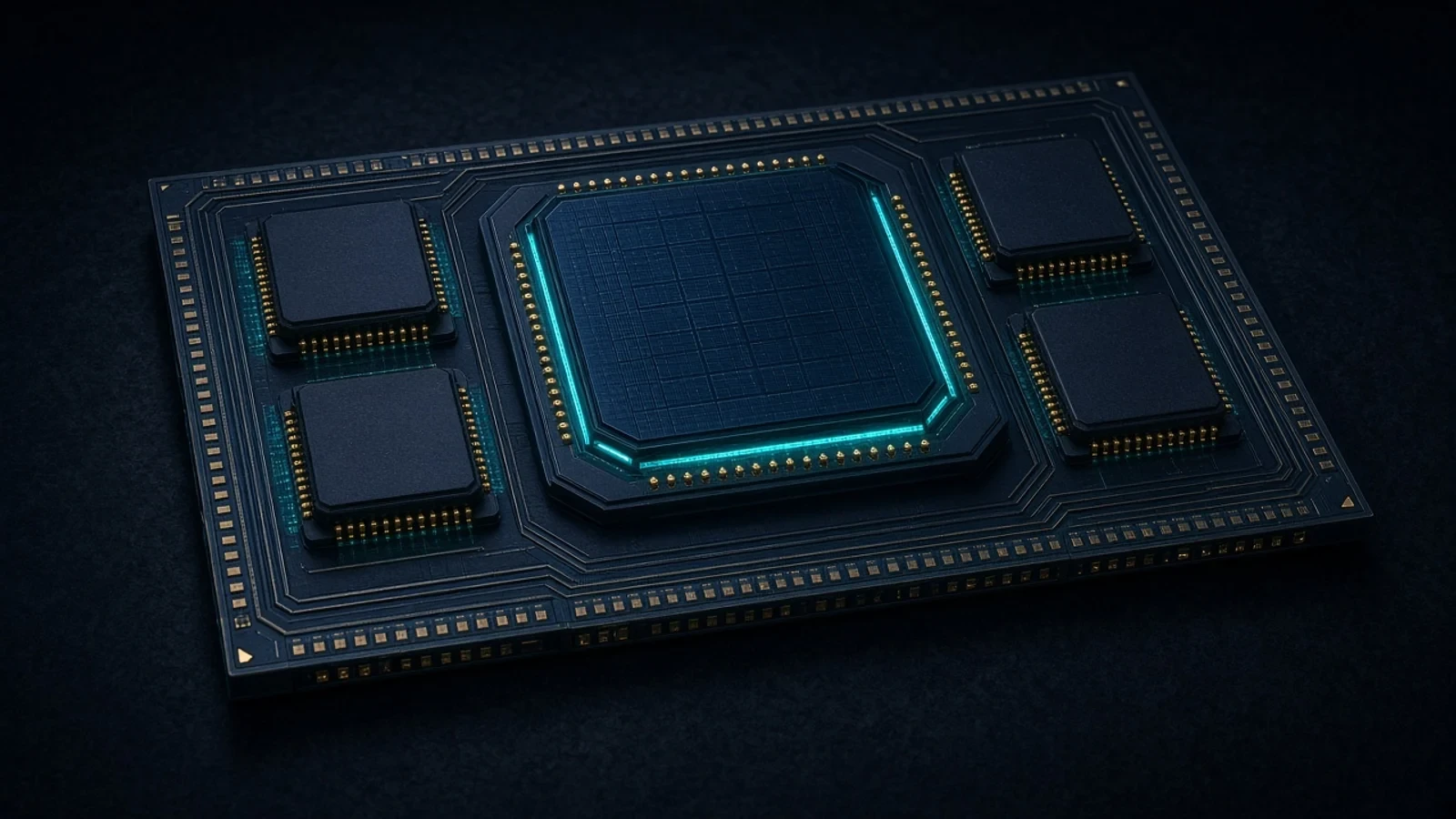
Apple Silicon is Apple’s fabless SoC platform. The M1 newsroom introduction defines a system-on-chip with CPU, GPU, Neural Engine, I/O and unified memory on a single package so those engines share one memory pool.
AI & HPCConsumer ElectronicsView Technology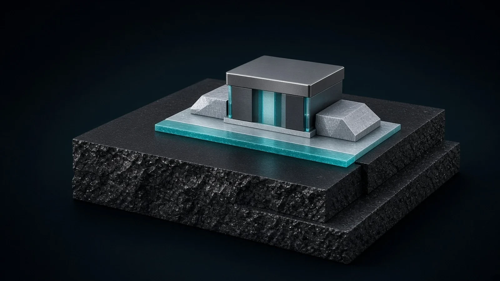
22FDX is GlobalFoundries’ 22 nm fully depleted SOI platform: a thin-body transistor on an insulating layer, targeting low-power, RF, automotive and IoT designs that do not need leading-edge GAA.
AutomotiveConsumer Electronics+2View Technology
FastConnect 7900 is a 6 nm single-chip connectivity system integrating Wi-Fi 7, Bluetooth and UWB, with High Band Simultaneous Multi-Link and companion RF front-end modules.
Consumer ElectronicsTelecommunications+1View Technology
Oryon is Qualcomm’s custom 64-bit CPU microarchitecture, including cache hierarchy, branch prediction, prefetch and later Flex Cache, designed in-house and scaled across Snapdragon platforms.
AutomotiveAI & HPC+2View Technology
Snapdragon X80 is Qualcomm's 5G Modem-RF system, combining the modem and RF front end, with 5G Advanced features and NB-NTN satellite support.
AutomotiveConsumer Electronics+1View Technology
Micron 3D NAND is a vertically stacked NAND flash technology family used as the semiconductor storage building block in data-center, client, mobile and automotive designs.
AutomotiveAI & HPC+2View Technology
Micron LPDDR is a low-power DRAM family for mobile, client, automotive and data-center designs that need high bandwidth at reduced power. LPDDR generations remain one technology line.
AutomotiveAI & HPC+2View Technology
Micron GDDR is a discrete graphics DRAM family spanning GDDR6, GDDR6X and GDDR7 generations for GPUs, gaming systems and AI inference accelerators.
AI & HPCConsumer ElectronicsView Technology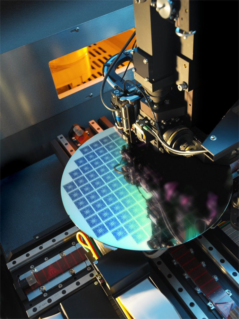
KLA overlay and dimensional metrology systems measure layer-to-layer alignment, critical dimensions and related pattern geometry. Distinct from defect inspection and review.
AutomotiveData Center+1View Technology
KLA wafer defect inspection and review systems used to find, classify and monitor particles and pattern defects. Distinct from overlay and dimensional metrology.
AutomotiveData Center+1View Technology
Lam Research wafer-process equipment category for thin-film deposition, plasma etch, strip, clean and related fabrication steps. SABRE ECD is listed separately.
Data CenterConsumer ElectronicsView Technology