Company
Japan
Semiconductor company that publishes CMOS image-sensor and depth-sensing technologies, including stacked CIS with Cu-Cu connection and SPAD dToF sensors.
2
Technologies
2
Technology Areas
4
Applications
Japan
Headquarters
Key technologies and platforms from this organization.
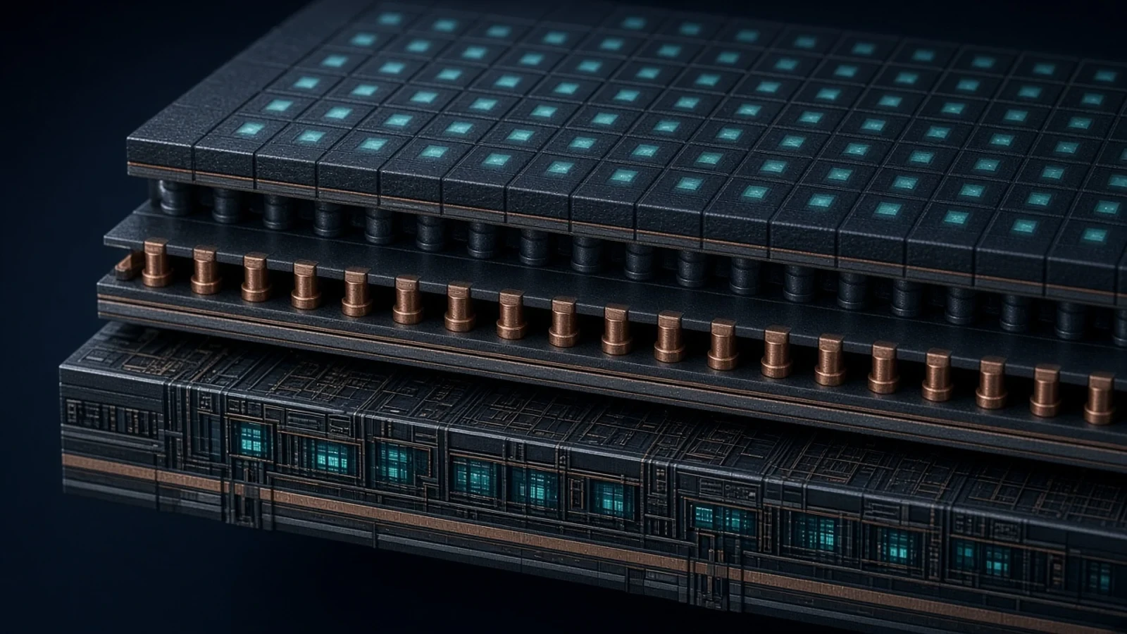
Sony’s stacked SPAD depth sensors use single-photon avalanche diodes and direct time-of-flight, with Cu-Cu pixel-to-logic connections, for long-range LiDAR and industrial ranging.
AutomotiveIndustrialView Details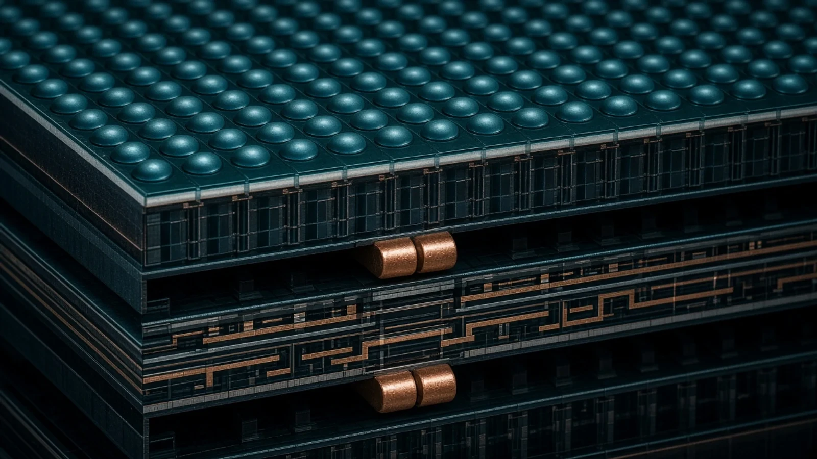
Sony’s stacked CMOS image sensor separates the pixel die from the logic die and joins them with Cu-Cu hybrid bonding, replacing TSVs. Official technology pages describe Cu-Cu as enabling denser, smaller, higher-function sensors.
AutomotiveIndustrialView DetailsKey focus areas and application domains for this organization.
Key themes and trends derived from the published technologies of this organization on Silicon Showcase.
2 published technologies in MEMS & Sensors.
Published technologies associated with Automotive and Industrial.
Published technologies associated with Consumer Electronics and Medical.