Skip to content
Silicon Showcase
CompaniesApplicationsTechnology AreasAbout
Submit Technology
Submit Technology
Silicon Showcase

Silicon Showcase™ is the global directory of semiconductor technologies, platforms and innovations from around the world.

  • Technologies
  • Technology Signals
  • Companies
  • Applications
  • Technology Areas
  • About Us
  • How It Works
  • Submit Technology
  • Contact Us
  • Privacy Policy
  • Terms of Use
  • Disclaimer

Explore

  • Technologies
  • Technology Signals
  • Companies
  • Applications
  • Technology Areas

About

  • About Us
  • How It Works
  • Submit Technology
  • Contact Us

Legal

  • Privacy Policy
  • Terms of Use
  • Disclaimer

© 2026 Silicon Showcase™. All rights reserved.

Explore. Compare. Innovate.

Silicon Showcase
CompaniesApplicationsTechnology AreasAbout
Submit Technology
Submit Technology
Silicon Showcase

Silicon Showcase™ is the global directory of semiconductor technologies, platforms and innovations from around the world.

  • Technologies
  • Technology Signals
  • Companies
  • Applications
  • Technology Areas
  • About Us
  • How It Works
  • Submit Technology
  • Contact Us
  • Privacy Policy
  • Terms of Use
  • Disclaimer

Explore

  • Technologies
  • Technology Signals
  • Companies
  • Applications
  • Technology Areas

About

  • About Us
  • How It Works
  • Submit Technology
  • Contact Us

Legal

  • Privacy Policy
  • Terms of Use
  • Disclaimer

© 2026 Silicon Showcase™. All rights reserved.

Explore. Compare. Innovate.

  1. Home
  2. /Technologies
  3. /Sony SPAD dToF Depth Sensing

SINGLE-PHOTON AVALANCHE DIODE

Single-photon avalanche diode pixels for direct time-of-flight
STACKED PIXEL AND

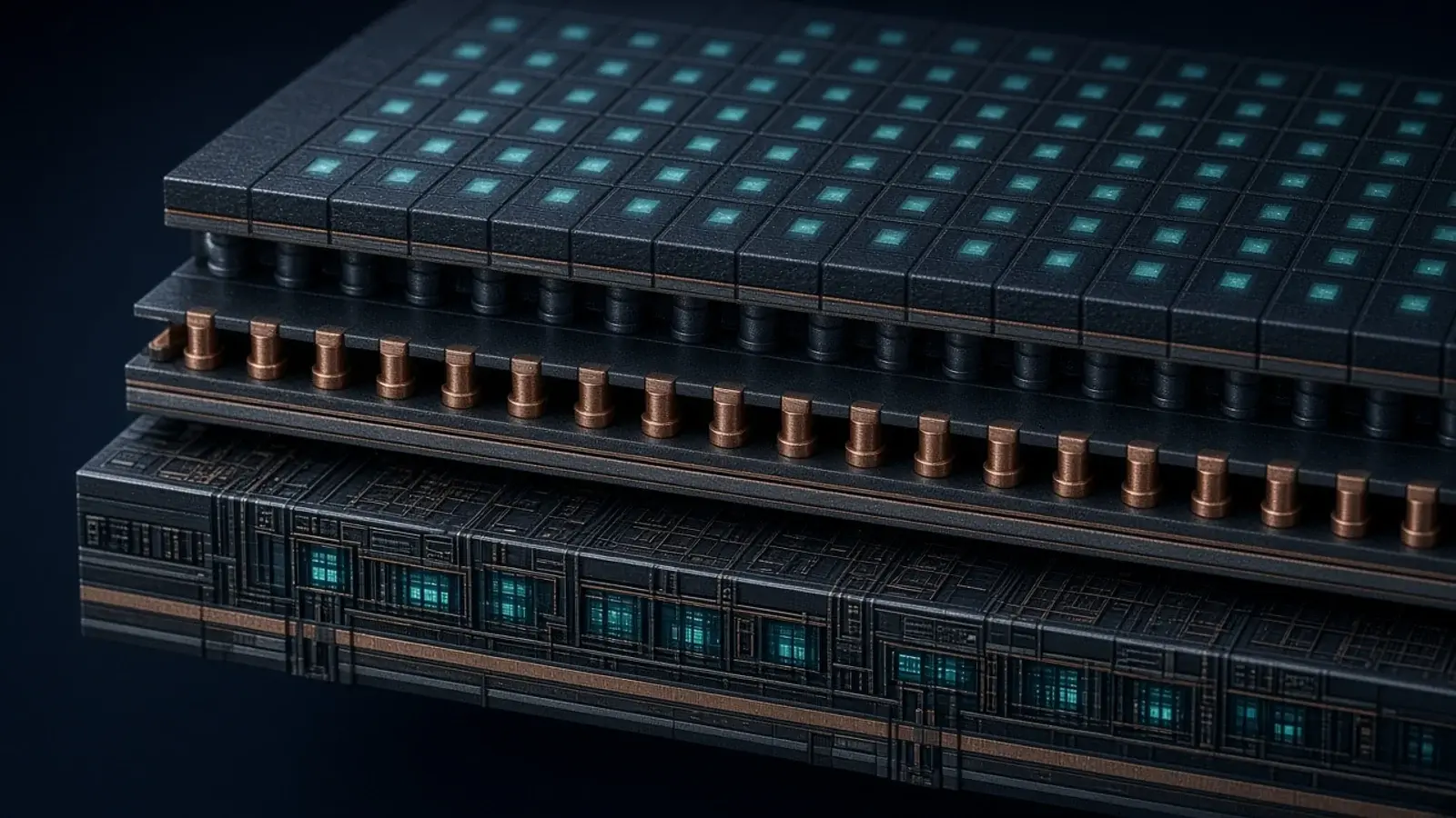
Stacked pixel and logic chips with Cu-Cu connections

APPLICATIONS

Automotive · Industrial

Silicon Showcase illustrative visual
Illustrative representation based on publicly available technical information.

SINGLE-PHOTON AVALANCHE DIODE

Single-photon avalanche diode pixels for direct time-of-flight

STACKED PIXEL AND

Stacked pixel and logic chips with Cu-Cu connections

APPLICATIONS

Automotive · Industrial

Public source

Sony SPAD dToF Depth Sensing

MEMS & Sensors

Sony SPAD dToF depth sensing is a publicly described sensor architecture that measures distance from the flight time of reflected light using single-photon avalanche diodes.

  • Automotive
  • Industrial
JapanView Official Source (opens in a new tab)

Silicon Showcase illustrative visual
Illustrative representation based on publicly available technical information.

Overview

Sony’s stacked SPAD depth sensors use single-photon avalanche diodes and direct time-of-flight, with Cu-Cu pixel-to-logic connections, for long-range LiDAR and industrial ranging.

Official Sony Semiconductor Solutions technology and product pages describe a stacked construction with Cu-Cu connections between a back-illuminated SPAD pixel chip and a logic chip that holds timing circuits. A 10 June 2025 news release describes a stacked SPAD depth sensor for automotive LiDAR. This listing records the SPAD/dToF architecture rather than IMX459 or IMX479 as separate rows. Stacked CIS Cu-Cu is listed separately as the imaging platform that shares bonding methods but not this detector physics. Pixel size and ranging claims should be confirmed on Sony’s current ToF pages.

Capabilities

Key characteristics associated with this technology.

  • Single-photon avalanche diode pixels for direct time-of-flight

  • Stacked pixel and logic chips with Cu-Cu connections

  • Official pages describe automotive LiDAR and industrial ranging uses

  • Not an IMX model-number catalog

Organization

Sony Semiconductor Solutions

Japan

View organization

Official resources

  • Sony ToF technologysony-semicon.com (opens in a new tab)
  • Sony automotive SPAD dToFsony-semicon.com (opens in a new tab)
  • Sony stacked SPAD depth sensor newssony-semicon.com (opens in a new tab)

Source & disclosure

Independent discovery listing. This profile was prepared from publicly available information published by the organization. For the latest and complete technical information, refer to the official company source.

Official source

sony-semicon.com (opens in a new tab)

Last source check

Sep 15, 2026

Notice something that needs updating?

Report a correction

Related Technologies

Explore other semiconductor technologies.

Design & IP

VS1111FESOC

Metering system-on-chip that Vervesemi describes as an analog front end integrated with a microcontroller for single-phase energy measurement.

IndustrialEnergyView Technology
Connectivity & RF

Vihaan-I Networking SoC

Aheesa's Vihaan-I is a RISC-V networking SoC for fiber broadband. First-pass silicon was announced in 2026, with production tape-out targeted for 2027.

AutomotiveIndustrialView Technology
Materials & Substrates

Advanced IC Photomasks

Photronics advanced IC photomasks are lithography reticles for integrated circuits, not a foundry node and not FPD masks.

AutomotiveAI & HPCView Technology

Power Semiconductors

AlphaSGT

AlphaSGT is Alpha and Omega’s shielded-gate trench MOSFET technology, not a GaN HEMT and not a power-module substrate.

AI & HPCData CenterView Technology