Skip to content
Silicon Showcase
CompaniesApplicationsTechnology AreasAbout
Submit Technology
Submit Technology
Silicon Showcase

Silicon Showcase™ is the global directory of semiconductor technologies, platforms and innovations from around the world.

  • Technologies
  • Technology Signals
  • Companies
  • Applications
  • Technology Areas
  • About Us
  • How It Works
  • Submit Technology
  • Contact Us
  • Privacy Policy
  • Terms of Use
  • Disclaimer

Explore

  • Technologies
  • Technology Signals
  • Companies
  • Applications
  • Technology Areas

About

  • About Us
  • How It Works
  • Submit Technology
  • Contact Us

Legal

  • Privacy Policy
  • Terms of Use
  • Disclaimer

© 2026 Silicon Showcase™. All rights reserved.

Explore. Compare. Innovate.

Silicon Showcase
CompaniesApplicationsTechnology AreasAbout
Submit Technology
Submit Technology
Silicon Showcase

Silicon Showcase™ is the global directory of semiconductor technologies, platforms and innovations from around the world.

  • Technologies
  • Technology Signals
  • Companies
  • Applications
  • Technology Areas
  • About Us
  • How It Works
  • Submit Technology
  • Contact Us
  • Privacy Policy
  • Terms of Use
  • Disclaimer

Explore

  • Technologies
  • Technology Signals
  • Companies
  • Applications
  • Technology Areas

About

  • About Us
  • How It Works
  • Submit Technology
  • Contact Us

Legal

  • Privacy Policy
  • Terms of Use
  • Disclaimer

© 2026 Silicon Showcase™. All rights reserved.

Explore. Compare. Innovate.

  1. Home
  2. /Companies
  3. /Applied Materials

Company

Applied Materials

United States|Santa Clara (HQ)

Materials engineering and wafer-fab equipment company that publishes semiconductor process platforms used to deposit, shape, modify and analyze materials on wafers.

  • Manufacturing Equipment
  • AI & HPC
  • Data Center
Visit Organization Website (opens in a new tab)

Source & Disclosure

Independent discovery listing based on publicly available information published by the organization.

Report a correction

2

Technologies

1

Technology Areas

2

Applications

United States

Headquarters

Technologies (2)

Key technologies and platforms from this organization.

Manufacturing Equipment

Applied Materials Endura PVD

Applied Materials Endura is an ultra-high-vacuum metallization platform used for physical vapor deposition and integrated multi-chamber sequences. Distinct from the Vistara wafer-manufacturing chassis.

AI & HPCData CenterView Details
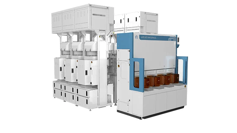
Manufacturing Equipment

Applied Materials Vistara

Modular semiconductor wafer-manufacturing chassis from Applied Materials for combining multiple chamber types on one system. Distinct from the Endura metallization platform.

AI & HPCData CenterView Details

Technology Footprint

Key focus areas and application domains for this organization.

Technology Areas (1)

  • Manufacturing Equipment

Applications (2)

  • AI & HPC
  • Data Center

Technology Signals

Key themes and trends derived from the published technologies of this organization on Silicon Showcase.

  • Manufacturing Equipment

    2 published technologies in Manufacturing Equipment.

  • AI & HPC and Data Center

    Published technologies associated with AI & HPC and Data Center.