Skip to content
Silicon Showcase
CompaniesApplicationsTechnology AreasAbout
Submit Technology
Submit Technology
Silicon Showcase

Silicon Showcase™ is the global directory of semiconductor technologies, platforms and innovations from around the world.

  • Technologies
  • Technology Signals
  • Companies
  • Applications
  • Technology Areas
  • About Us
  • How It Works
  • Submit Technology
  • Contact Us
  • Privacy Policy
  • Terms of Use
  • Disclaimer

Explore

  • Technologies
  • Technology Signals
  • Companies
  • Applications
  • Technology Areas

About

  • About Us
  • How It Works
  • Submit Technology
  • Contact Us

Legal

  • Privacy Policy
  • Terms of Use
  • Disclaimer

© 2026 Silicon Showcase™. All rights reserved.

Explore. Compare. Innovate.

Silicon Showcase
CompaniesApplicationsTechnology AreasAbout
Submit Technology
Submit Technology
Silicon Showcase

Silicon Showcase™ is the global directory of semiconductor technologies, platforms and innovations from around the world.

  • Technologies
  • Technology Signals
  • Companies
  • Applications
  • Technology Areas
  • About Us
  • How It Works
  • Submit Technology
  • Contact Us
  • Privacy Policy
  • Terms of Use
  • Disclaimer

Explore

  • Technologies
  • Technology Signals
  • Companies
  • Applications
  • Technology Areas

About

  • About Us
  • How It Works
  • Submit Technology
  • Contact Us

Legal

  • Privacy Policy
  • Terms of Use
  • Disclaimer

© 2026 Silicon Showcase™. All rights reserved.

Explore. Compare. Innovate.

  1. Home
  2. /Technology Signals
  3. /CFET & Vertically Stacked Transistors

Emerging Signal

CFET & Vertically Stacked Transistors

Vertically stacked complementary transistors are extending logic scaling beyond conventional gate-all-around architectures.
Manufacturing EquipmentMaterials & SubstratesFoundry / Process
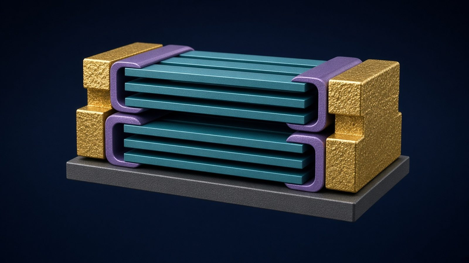
Illustrative vertically stacked transistor visual. Original Silicon Showcase illustration.

What It Is

A complementary FET stacks n-type and p-type transistors vertically instead of placing them side by side. Device research treats this architecture as a candidate for continuing logic-cell scaling after gate-all-around nanosheet transistors. Two integration paths are under study: building the stack in one process flow, or forming the upper device on a transferred layer.

Why It Matters

Side-by-side n-type and p-type devices set a limit on how short a standard cell can be. Vertical stacking is being explored because it can take that separation out of the cell height. The tradeoff is a more complex process, including new ways to contact each device.

What To Watch

Watch how monolithic and sequential integration approaches develop, how the stacked devices are contacted and powered, and which channel materials are evaluated for the upper and lower transistors.

Explore the Ecosystem

Technology Areas

Manufacturing EquipmentMaterials & SubstratesFoundry / Process

Sources & Further Reading

  • imec · Primary

    Complementary FET (CFET) on the logic technology roadmap

    Visit source (opens in a new tab)
  • imec

    Chip scaling roadmap

    Visit source (opens in a new tab)

Technology Signals are editorial summaries based on publicly available sources. Technical claims remain attributable to their original sources.
