Skip to content
Silicon Showcase
CompaniesApplicationsTechnology AreasAbout
Submit Technology
Submit Technology
Silicon Showcase

Silicon Showcase™ is the global directory of semiconductor technologies, platforms and innovations from around the world.

  • Technologies
  • Technology Signals
  • Companies
  • Applications
  • Technology Areas
  • About Us
  • How It Works
  • Submit Technology
  • Contact Us
  • Privacy Policy
  • Terms of Use
  • Disclaimer

Explore

  • Technologies
  • Technology Signals
  • Companies
  • Applications
  • Technology Areas

About

  • About Us
  • How It Works
  • Submit Technology
  • Contact Us

Legal

  • Privacy Policy
  • Terms of Use
  • Disclaimer

© 2026 Silicon Showcase™. All rights reserved.

Explore. Compare. Innovate.

Silicon Showcase
CompaniesApplicationsTechnology AreasAbout
Submit Technology
Submit Technology
Silicon Showcase

Silicon Showcase™ is the global directory of semiconductor technologies, platforms and innovations from around the world.

  • Technologies
  • Technology Signals
  • Companies
  • Applications
  • Technology Areas
  • About Us
  • How It Works
  • Submit Technology
  • Contact Us
  • Privacy Policy
  • Terms of Use
  • Disclaimer

Explore

  • Technologies
  • Technology Signals
  • Companies
  • Applications
  • Technology Areas

About

  • About Us
  • How It Works
  • Submit Technology
  • Contact Us

Legal

  • Privacy Policy
  • Terms of Use
  • Disclaimer

© 2026 Silicon Showcase™. All rights reserved.

Explore. Compare. Innovate.

  1. Home
  2. /Technology Areas
  3. /Materials & Substrates

Technology Area

Materials & Substrates

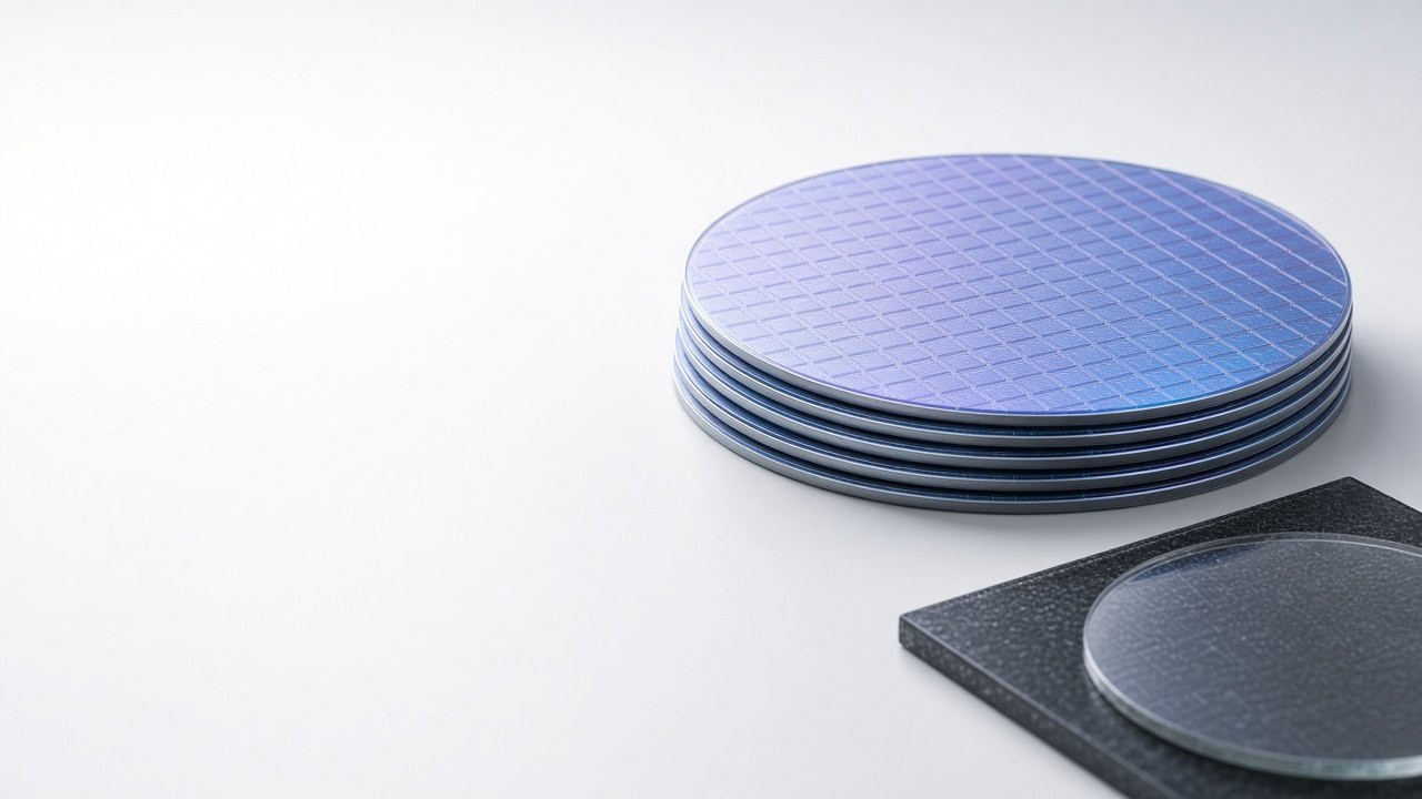
Wafers, substrates, process materials and related material platforms.

Technologies

13

Technologies

Companies

13

Companies

Applications

9

Applications

About Materials & Substrates

Materials and substrates are the wafers, films and package bases on which semiconductor devices are built. The area includes silicon and compound-semiconductor wafers, epitaxial layers, dielectrics and metals, and organic or ceramic package substrates used in fabrication and assembly.

Key Segments

  • Silicon Wafers
  • Wide-Bandgap Substrates
  • Compound Semiconductors
  • Dielectrics & Films
  • Package Substrates

Why It Matters

  • Device performance foundation
  • Wide-bandgap capability
  • Improved material reliability
  • Packaging and assembly support

Explore Technologies

Discover technologies, solutions and innovations in this area.
View all technologies
Materials & Substrates

Advanced Deposition Materials Platform

Entegris Advanced Deposition Materials is a process-materials platform for precursor and deposition chemistries used in semiconductor manufacturing.

AutomotiveAI & HPCData Center+1View Technology
Materials & Substrates

Advanced IC Photomasks

Photronics advanced IC photomasks are lithography reticles for integrated circuits, not a foundry node and not FPD masks.

AutomotiveAI & HPCConsumer ElectronicsView Technology
Materials & Substrates

Emblem Next-Gen CMP Pad Platform

Qnity Emblem is a next-generation CMP pad platform for advanced-node planarization, not a polishing tool.

AI & HPCData CenterConsumer ElectronicsView Technology

Related Applications

Key application areas leveraging these technologies.

View all applications
AutomotiveAI & HPCData CenterIndustrialConsumer ElectronicsTelecommunicationsAerospace & DefenseEnergyIoT

Technology area visuals are illustrative representations.