Skip to content
Silicon Showcase
CompaniesApplicationsTechnology AreasAbout
Submit Technology
Submit Technology
Silicon Showcase

Silicon Showcase™ is the global directory of semiconductor technologies, platforms and innovations from around the world.

  • Technologies
  • Technology Signals
  • Companies
  • Applications
  • Technology Areas
  • About Us
  • How It Works
  • Submit Technology
  • Contact Us
  • Privacy Policy
  • Terms of Use
  • Disclaimer

Explore

  • Technologies
  • Technology Signals
  • Companies
  • Applications
  • Technology Areas

About

  • About Us
  • How It Works
  • Submit Technology
  • Contact Us

Legal

  • Privacy Policy
  • Terms of Use
  • Disclaimer

© 2026 Silicon Showcase™. All rights reserved.

Explore. Compare. Innovate.

Silicon Showcase
CompaniesApplicationsTechnology AreasAbout
Submit Technology
Submit Technology
Silicon Showcase

Silicon Showcase™ is the global directory of semiconductor technologies, platforms and innovations from around the world.

  • Technologies
  • Technology Signals
  • Companies
  • Applications
  • Technology Areas
  • About Us
  • How It Works
  • Submit Technology
  • Contact Us
  • Privacy Policy
  • Terms of Use
  • Disclaimer

Explore

  • Technologies
  • Technology Signals
  • Companies
  • Applications
  • Technology Areas

About

  • About Us
  • How It Works
  • Submit Technology
  • Contact Us

Legal

  • Privacy Policy
  • Terms of Use
  • Disclaimer

© 2026 Silicon Showcase™. All rights reserved.

Explore. Compare. Innovate.

  1. Home
  2. /Technology Areas
  3. /Foundry / Process

Technology Area

Foundry / Process

Foundry process nodes and specialty wafer-process platforms.

Technologies

11

Technologies

Companies

11

Companies

Applications

9

Applications

About Foundry / Process

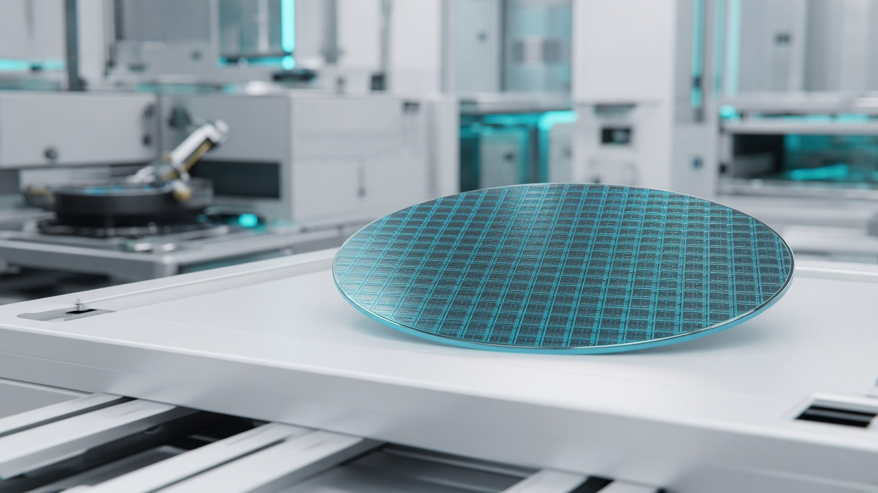
Foundry / Process covers semiconductor process technologies whose primary identity is a published foundry node or process platform — including logic CMOS, FD-SOI, analog/RF BiCMOS and BCD, compound III-V, and 3D or embedded-memory process offerings. Listings describe the process platform rather than manufacturing equipment, starting wafers, packaging, licensed IP, or finished power devices.

Key Segments

  • Logic Process Nodes
  • FD-SOI & Specialty CMOS
  • Analog, BCD & RF Process
  • Compound / III-V Foundry
  • 3D & Embedded Memory Process

Why It Matters

  • Advanced logic scaling
  • Specialty process options
  • Mixed-signal and RF integration
  • Volume manufacturing access

Explore Technologies

Discover technologies, solutions and innovations in this area.
View all technologies
Foundry / Process

22ULP/ULL

UMC 22ULP/ULL is the foundry’s 22-nanometer ultra-low-power / ultra-low-leakage logic process platform.

AutomotiveConsumer ElectronicsTelecommunications+1View Technology
Foundry / Process

28nm HKMG Process

SMIC 28nm HKMG is the foundry’s published 28-nanometer high-k metal-gate logic process, documented in SMIC newsroom coverage.

AI & HPCConsumer ElectronicsTelecommunicationsView Technology
Foundry / Process

3D AI Foundry

Powerchip 3D AI Foundry is a wafer-on-wafer logic/memory stacking foundry offering, parked in Advanced Packaging because Foundry / Process does not yet exist.

AutomotiveAI & HPCData CenterView Technology

Related Applications

Key application areas leveraging these technologies.

View all applications
AutomotiveAI & HPCData CenterIndustrialConsumer ElectronicsTelecommunicationsAerospace & DefenseEnergyIoT

Technology area visuals are illustrative representations.