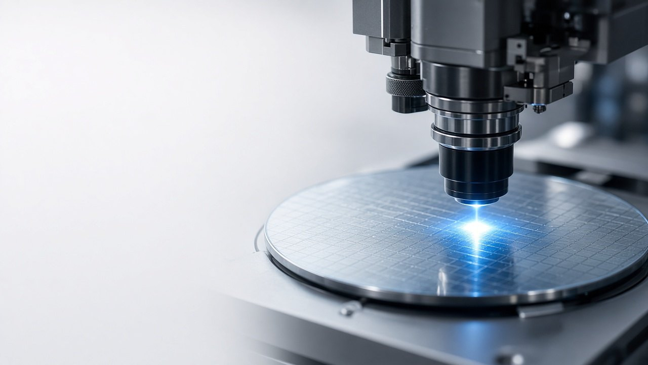
Technology Area
Test, measurement, inspection and metrology capabilities across the semiconductor flow.
13
Technologies
12
Companies
8
Applications
Test and inspection covers measurement, metrology and electrical test used to characterize wafers, packages and finished devices. Optical and e-beam inspection, overlay and film metrology, probe and final test, and failure analysis confirm process control and device behavior.
Discover technologies, solutions and innovations in this area.
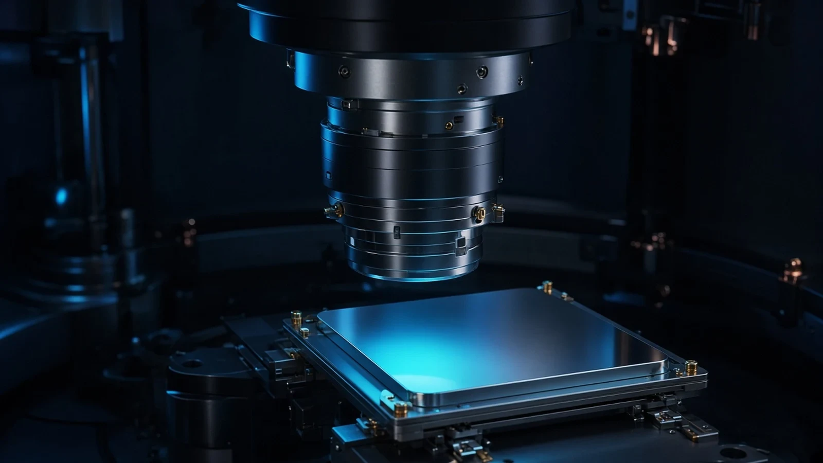
Lasertec ACTIS is an actinic EUV photomask inspection platform for high-volume EUV mask qualification.
AI & HPCData CenterConsumer ElectronicsView Technology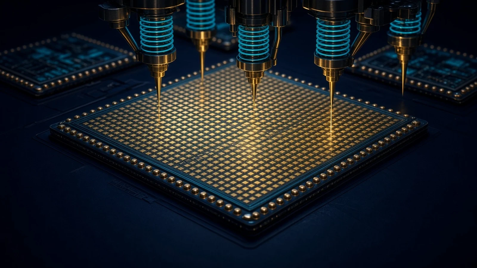
FormFactor composite-metal MEMS is a wafer-probe-card technology, not a MEMS sensor product.
AutomotiveAI & HPCData CenterView Technology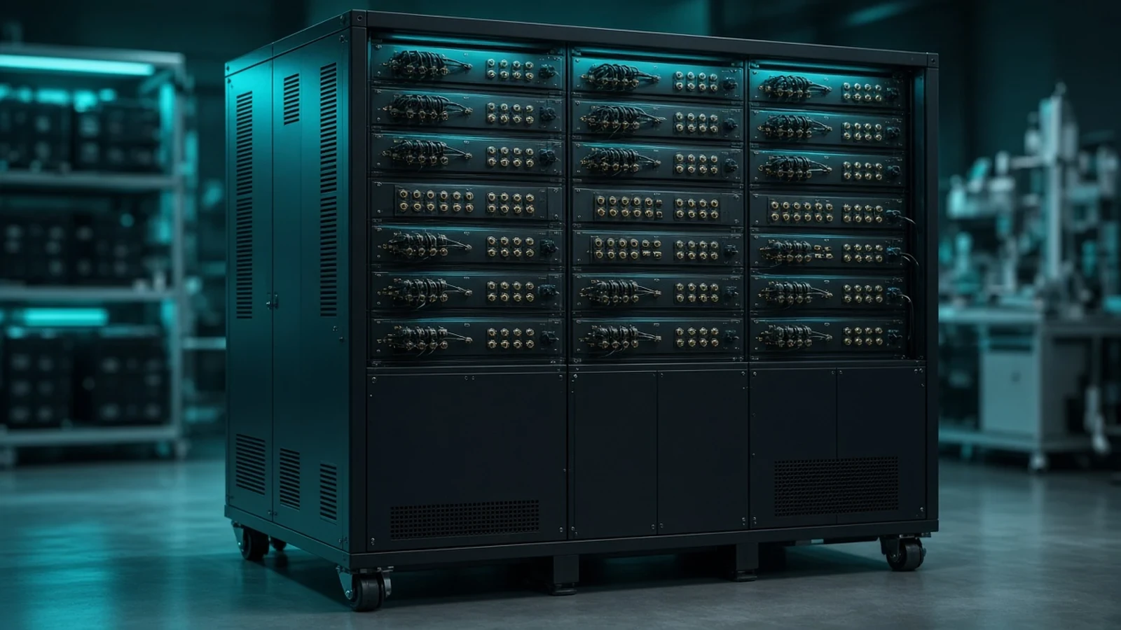
Cohu Diamondx is semiconductor ATE instrumentation, not a handler and not a probe card.
AutomotiveAI & HPCIndustrial+1View TechnologyKey application areas leveraging these technologies.
Technology area visuals are illustrative representations.