Discover 169 technologies from leading innovators around the world.
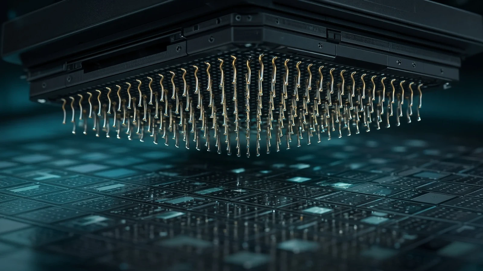
Micronics Japan MEMS-SP is a MEMS probe-card technology for wafer test, not a handler and not a packaged-device socket.
AutomotiveAI & HPC+1View Technology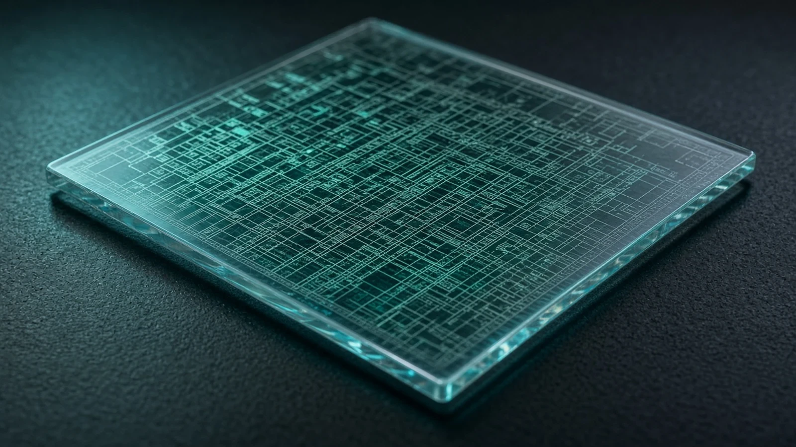
Tekscend semiconductor photomasks are lithography reticles, not a foundry process node and not a mask writer.
AutomotiveAI & HPC+1View Technology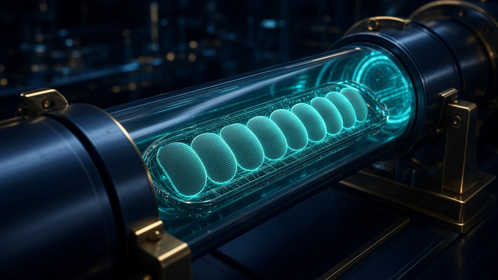
Kokusai Batch ALD combines atomic-layer deposition with multi-wafer batch furnaces for 3D device films.
AI & HPCData Center+1View Technology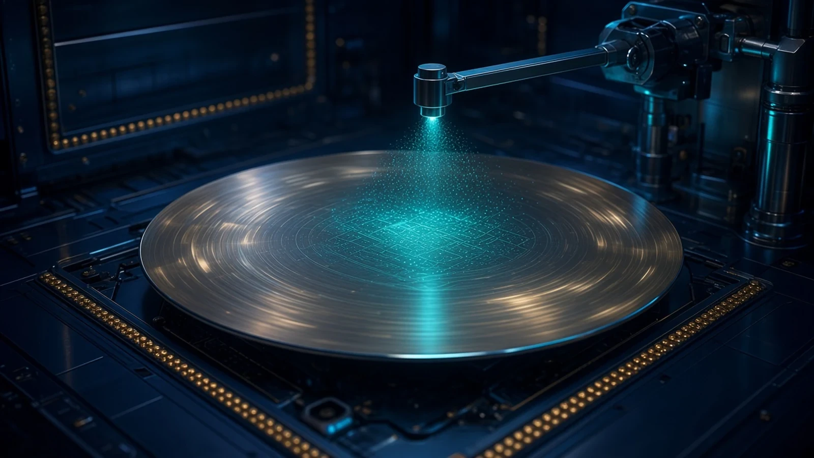
SCREEN SU Series is a single-wafer cleaning equipment family, currently described through SU-3400.
AutomotiveAI & HPC+1View Technology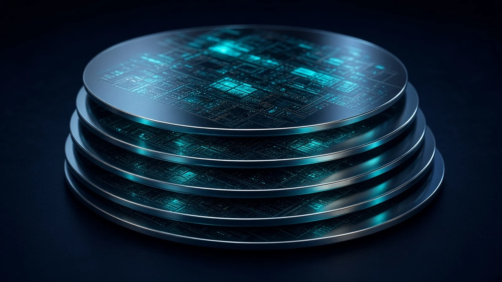
SUMCO Advanced Silicon Wafers are polished and specialty silicon starting substrates, including epitaxial, annealed and SOI wafers.
AutomotiveAI & HPC+2View Technology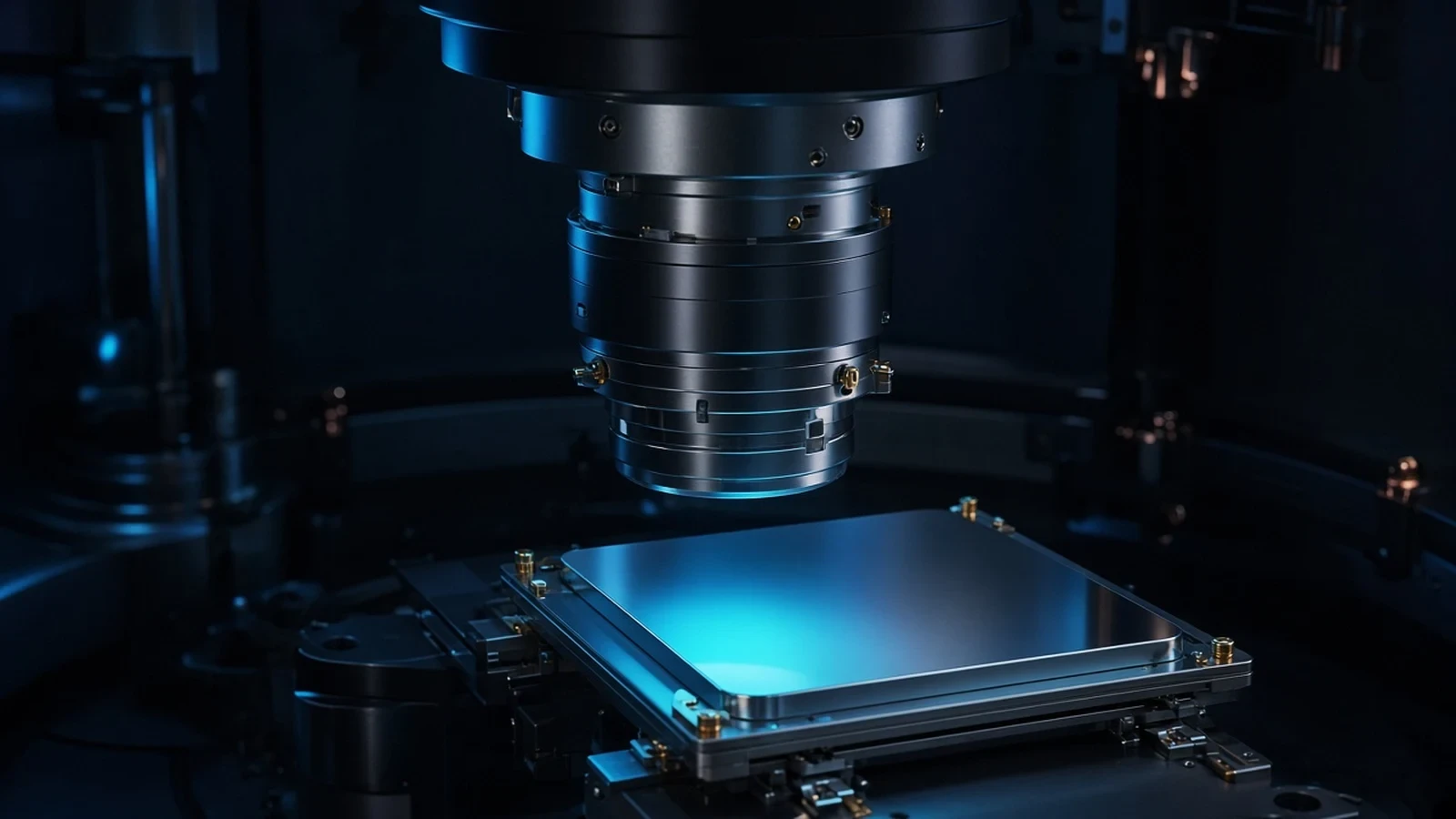
Lasertec ACTIS is an actinic EUV photomask inspection platform for high-volume EUV mask qualification.
AI & HPCData Center+1View Technology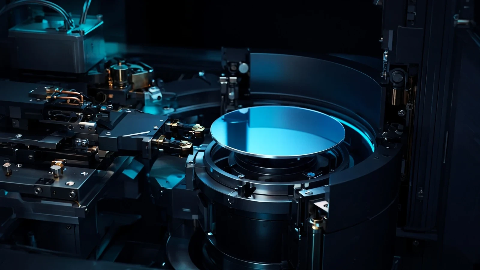
Tokyo Electron CLEAN TRACK LITHIUS is a coater/developer track platform used with lithography tools in high-volume wafer fabrication.
AutomotiveAI & HPC+2View Technology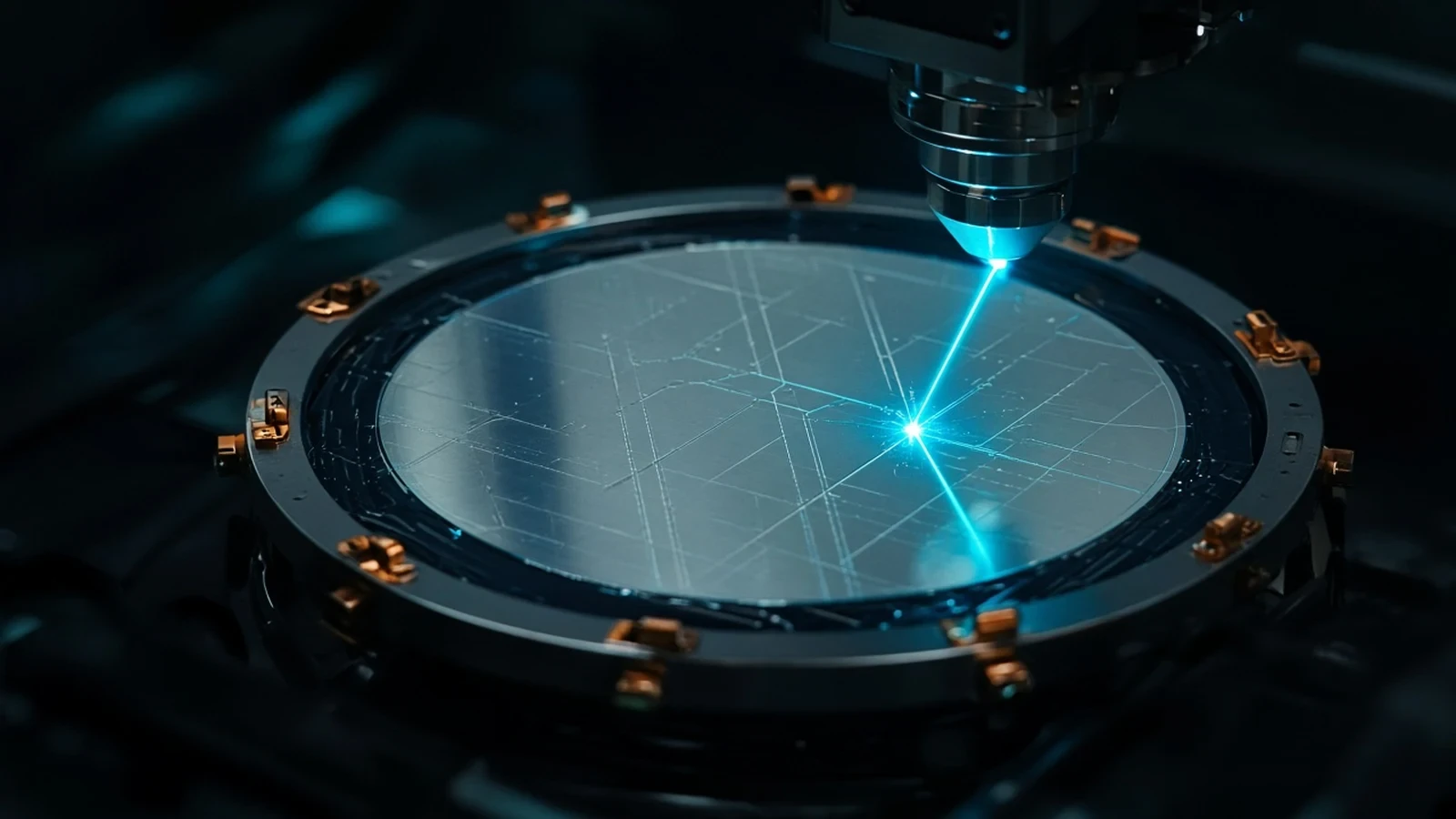
DISCO DBG with DAF laser cut is a dicing-before-grinding process that laser-cuts die-attach film during wafer thinning.
AutomotiveAI & HPC+1View Technology
Renesas R-Car is an automotive system-on-chip platform for ADAS, cockpit and vehicle compute, not a standalone data-center accelerator architecture.
AutomotiveAI & HPCView Technology
Advantest V93000 EXA Scale is a flagship SoC automatic test equipment platform for high-volume digital, mixed-signal and high-speed I/O devices.
AutomotiveAI & HPC+2View Technology