Skip to content
Silicon Showcase
CompaniesApplicationsTechnology AreasAbout
Submit Technology
Submit Technology
Silicon Showcase

Silicon Showcase™ is the global directory of semiconductor technologies, platforms and innovations from around the world.

  • Technologies
  • Technology Signals
  • Companies
  • Applications
  • Technology Areas
  • About Us
  • How It Works
  • Submit Technology
  • Contact Us
  • Privacy Policy
  • Terms of Use
  • Disclaimer

Explore

  • Technologies
  • Technology Signals
  • Companies
  • Applications
  • Technology Areas

About

  • About Us
  • How It Works
  • Submit Technology
  • Contact Us

Legal

  • Privacy Policy
  • Terms of Use
  • Disclaimer

© 2026 Silicon Showcase™. All rights reserved.

Explore. Compare. Innovate.

Silicon Showcase
CompaniesApplicationsTechnology AreasAbout
Submit Technology
Submit Technology
Silicon Showcase

Silicon Showcase™ is the global directory of semiconductor technologies, platforms and innovations from around the world.

  • Technologies
  • Technology Signals
  • Companies
  • Applications
  • Technology Areas
  • About Us
  • How It Works
  • Submit Technology
  • Contact Us
  • Privacy Policy
  • Terms of Use
  • Disclaimer

Explore

  • Technologies
  • Technology Signals
  • Companies
  • Applications
  • Technology Areas

About

  • About Us
  • How It Works
  • Submit Technology
  • Contact Us

Legal

  • Privacy Policy
  • Terms of Use
  • Disclaimer

© 2026 Silicon Showcase™. All rights reserved.

Explore. Compare. Innovate.

  1. Home
  2. /Technology Signals
  3. /Backside Power Delivery

Emerging Signal

Backside Power Delivery

Backside power networks separate power delivery from signal routing to improve density, efficiency and scaling at advanced nodes.
Manufacturing EquipmentFoundry / ProcessPower Semiconductors
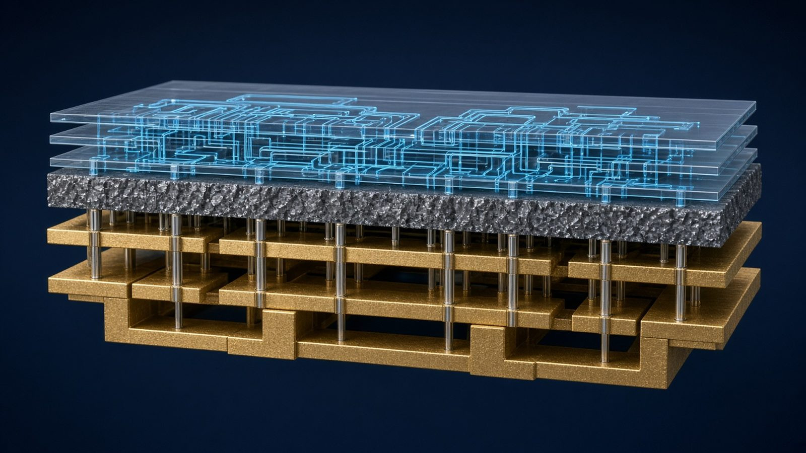
Illustrative backside power delivery visual. Original Silicon Showcase illustration.

What It Is

Backside power delivery moves the power distribution network to the reverse side of a thinned wafer, leaving the front side available for signal routing. Backside metals connect to the transistors through fine vias, so power and signal no longer have to share the same routing layers.

Why It Matters

At advanced nodes, dense signal routing and low-resistance power delivery compete for the same metal stack. Separating those networks is one approach under development for further logic scaling and for supplying power to dense devices.

What To Watch

Watch which process flows place power on the wafer backside, how those flows are combined with gate-all-around transistors and advanced packaging, and how design tools represent a backside power network.

Explore the Ecosystem

Technology Areas

Manufacturing EquipmentFoundry / ProcessPower Semiconductors

Sources & Further Reading

  • imec · Primary

    Backside power delivery

    Visit source (opens in a new tab)
  • imec

    Building blocks for a backside power delivery network

    Visit source (opens in a new tab)

Technology Signals are editorial summaries based on publicly available sources. Technical claims remain attributable to their original sources.
