Discover 169 technologies from leading innovators around the world.
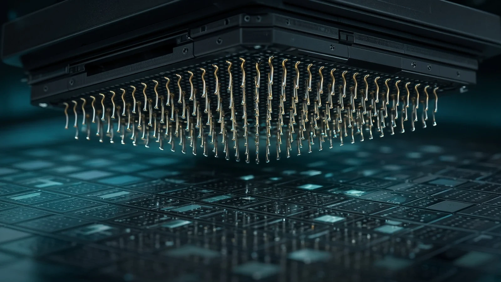
Micronics Japan MEMS-SP is a MEMS probe-card technology for wafer test, not a handler and not a packaged-device socket.
AutomotiveAI & HPCConsumer ElectronicsView Technology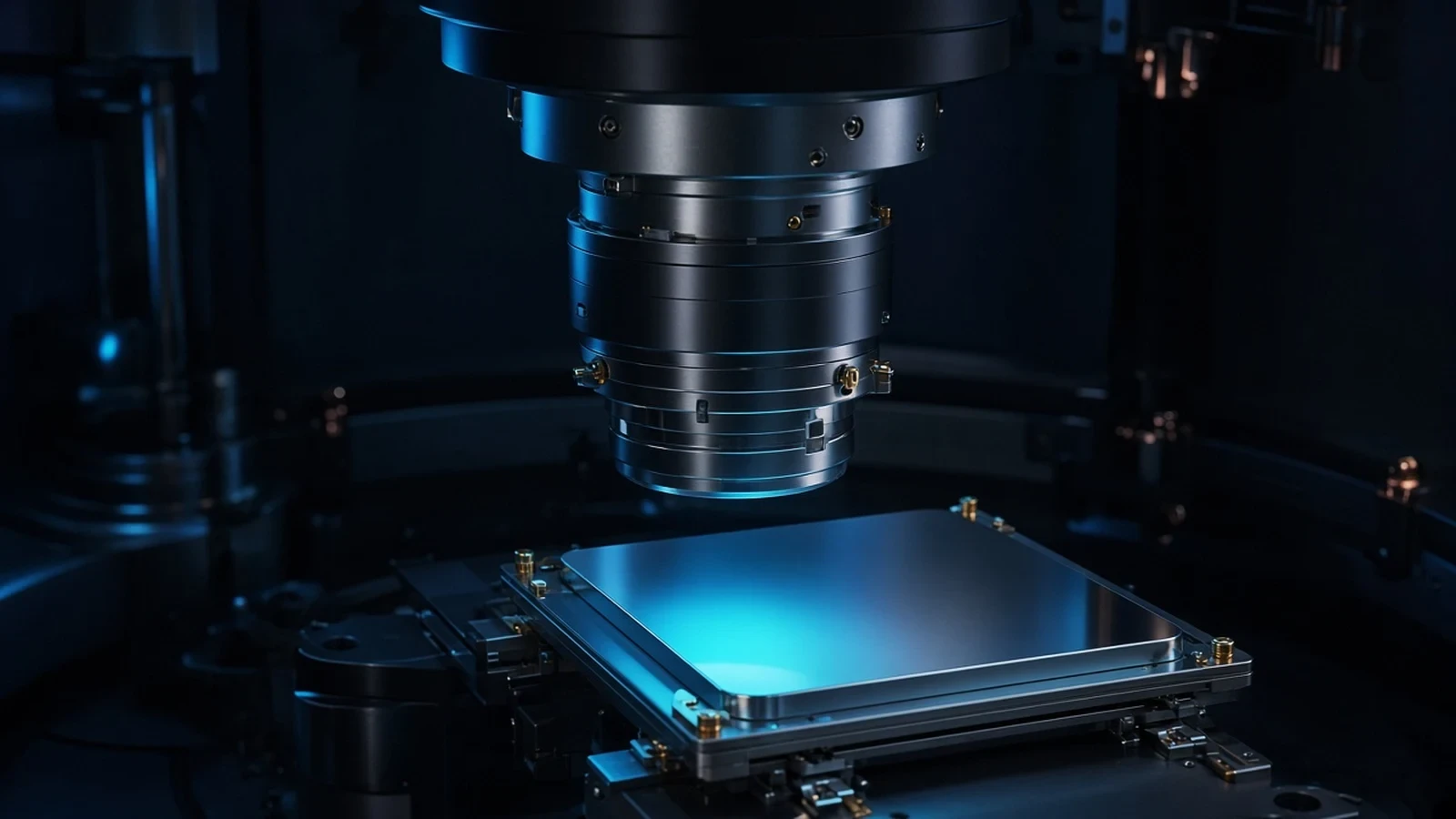
Lasertec ACTIS is an actinic EUV photomask inspection platform for high-volume EUV mask qualification.
AI & HPCData CenterConsumer ElectronicsView Technology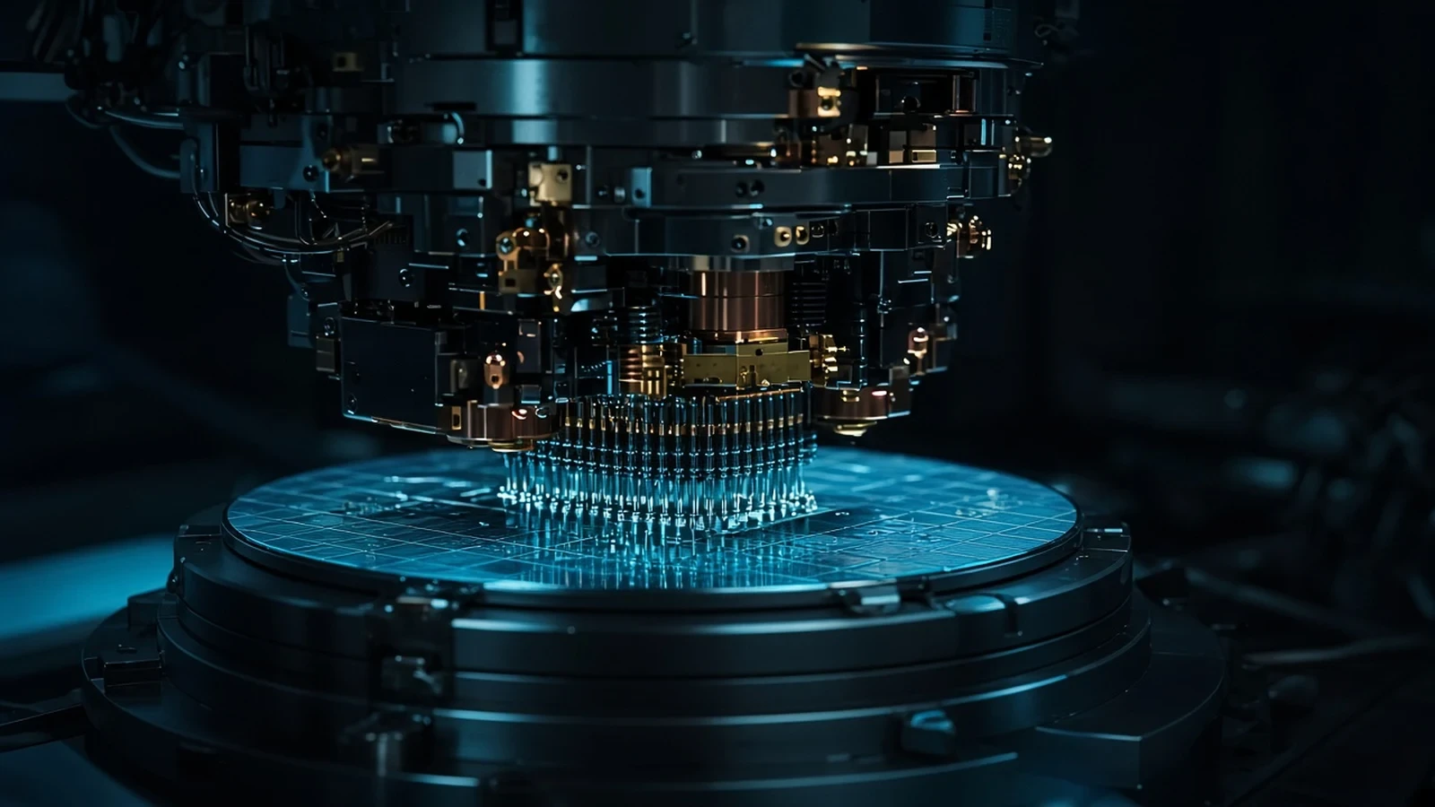
Advantest V93000 EXA Scale is a flagship SoC automatic test equipment platform for high-volume digital, mixed-signal and high-speed I/O devices.
AutomotiveAI & HPCData Center+1View Technology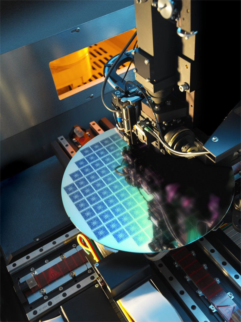
KLA overlay and dimensional metrology systems measure layer-to-layer alignment, critical dimensions and related pattern geometry. Distinct from defect inspection and review.
AutomotiveData CenterConsumer ElectronicsView Technology
KLA wafer defect inspection and review systems used to find, classify and monitor particles and pattern defects. Distinct from overlay and dimensional metrology.
AutomotiveData CenterConsumer ElectronicsView Technology