Discover 169 technologies from leading innovators around the world.
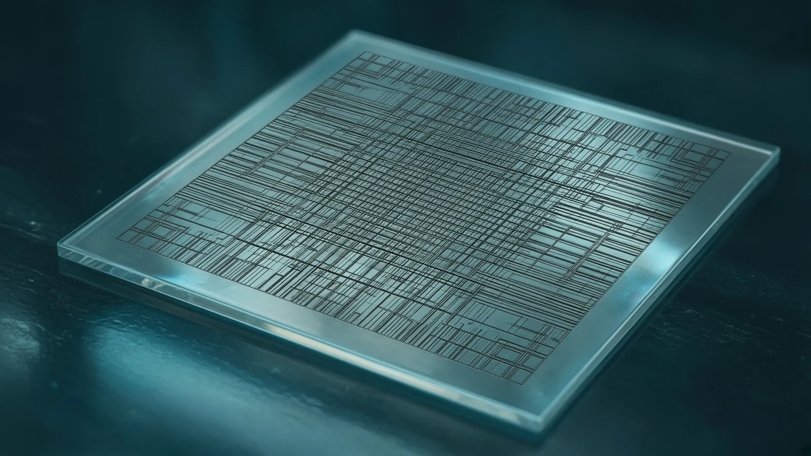
Photronics advanced IC photomasks are lithography reticles for integrated circuits, not a foundry node and not FPD masks.
AutomotiveAI & HPCConsumer ElectronicsView Technology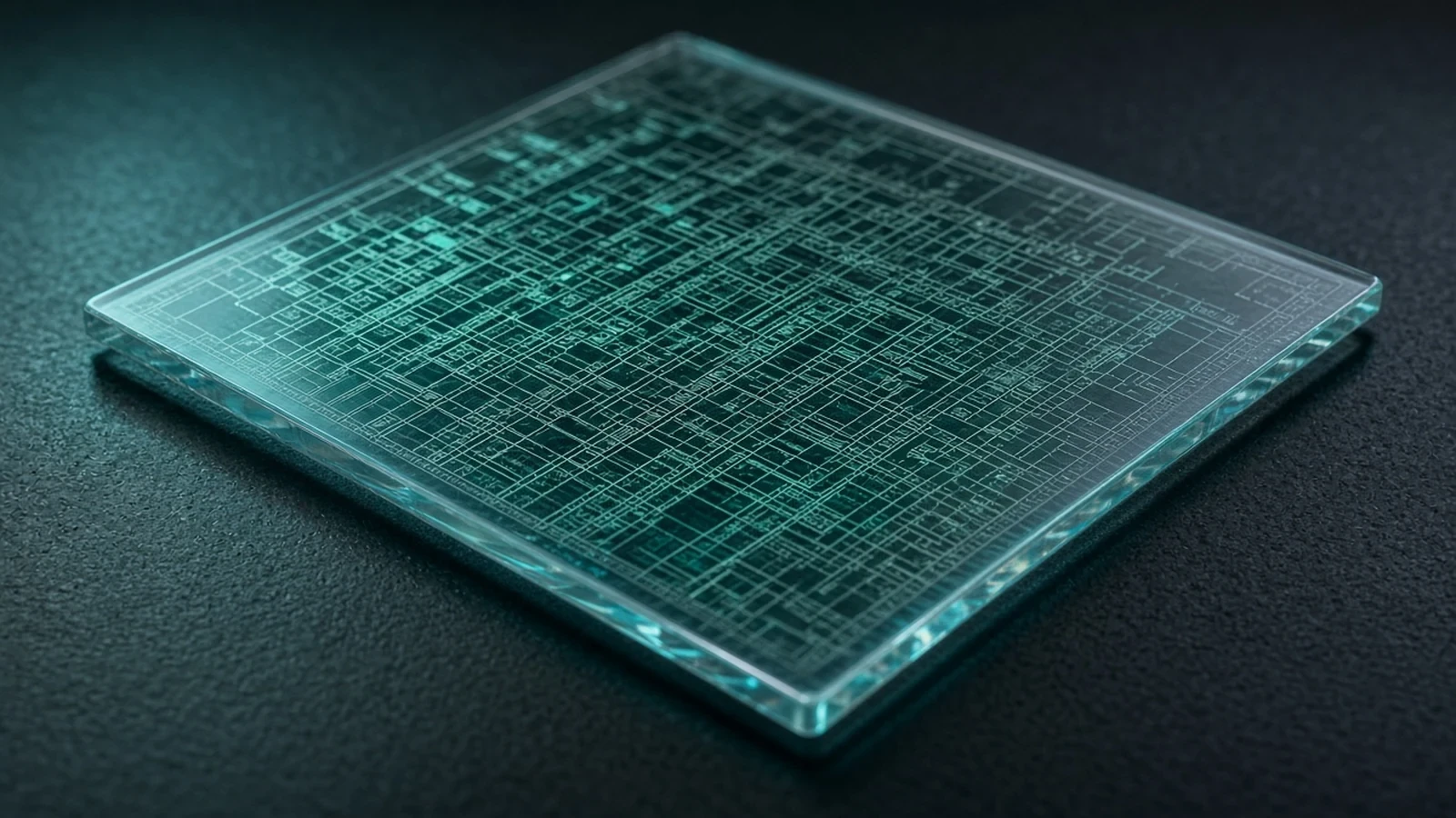
Tekscend semiconductor photomasks are lithography reticles, not a foundry process node and not a mask writer.
AutomotiveAI & HPCConsumer ElectronicsView Technology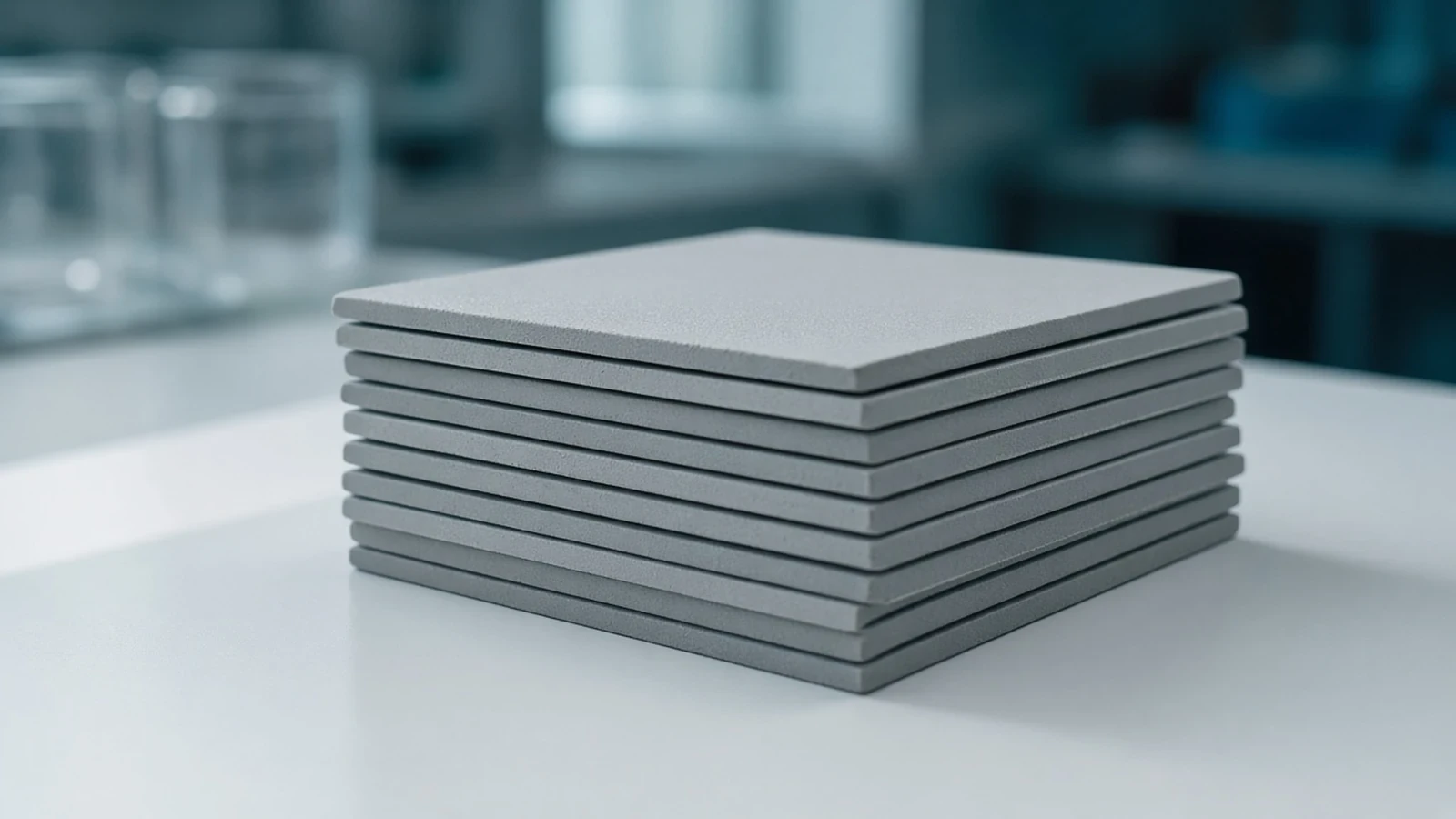
MARUWA silicon-nitride substrates are ceramic power-module boards, not a silicon wafer and not a packaged MOSFET.
AutomotiveIndustrialEnergyView Technology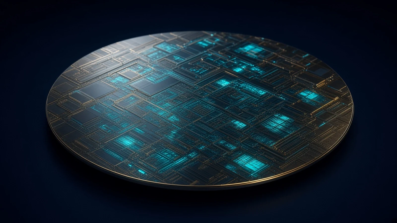
GlobalWafers Silicon Wafers are the company's silicon starting substrates, including annealed, epitaxial, SOI and diffusion wafers.
AutomotiveAI & HPCIndustrial+1View Technology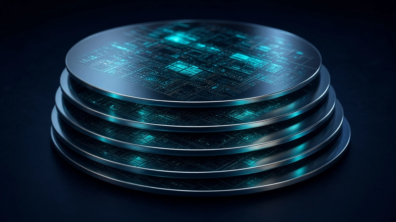
SUMCO Advanced Silicon Wafers are polished and specialty silicon starting substrates, including epitaxial, annealed and SOI wafers.
AutomotiveAI & HPCData Center+1View Technology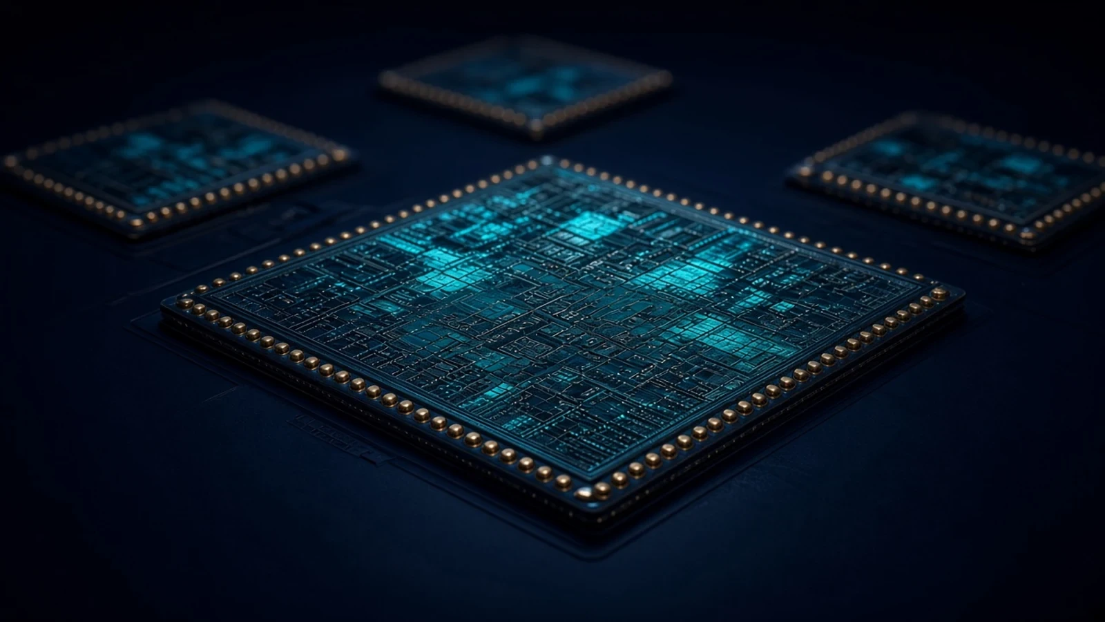
AT&S high-performance IC substrates are build-up package substrates that connect advanced processors to system boards, not generic PCBs and not OSAT assembly.
AutomotiveAI & HPCData Center+1View Technology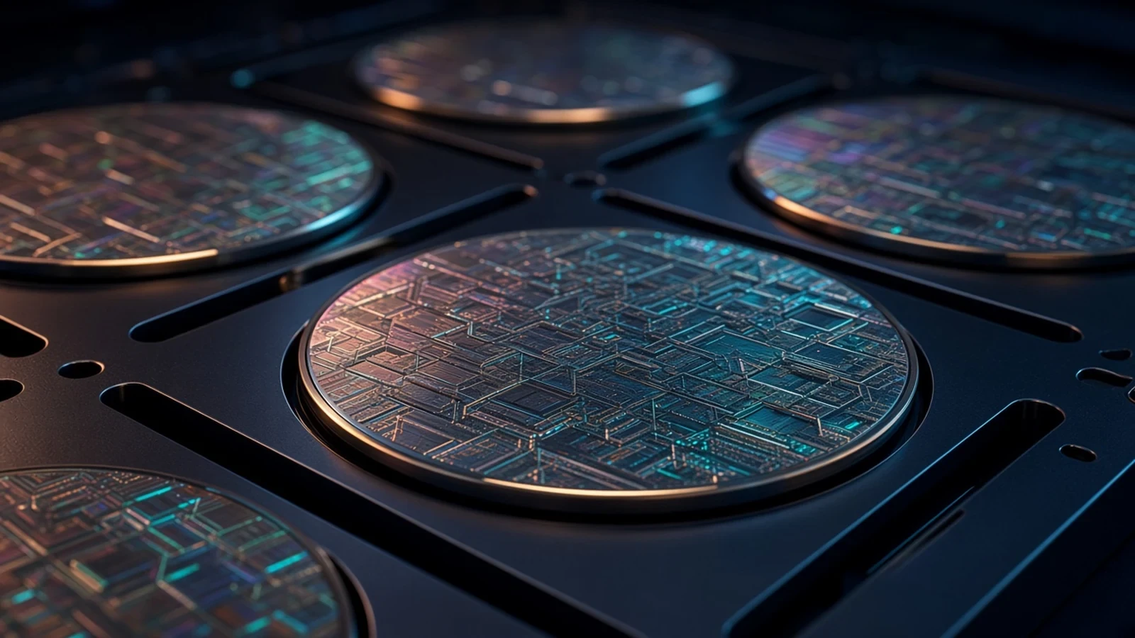
Coherent’s III-V epitaxial wafer platform supplies compound-semiconductor epi wafers for photonic and RF devices, not industrial laser systems.
AutomotiveData CenterIndustrial+1View Technology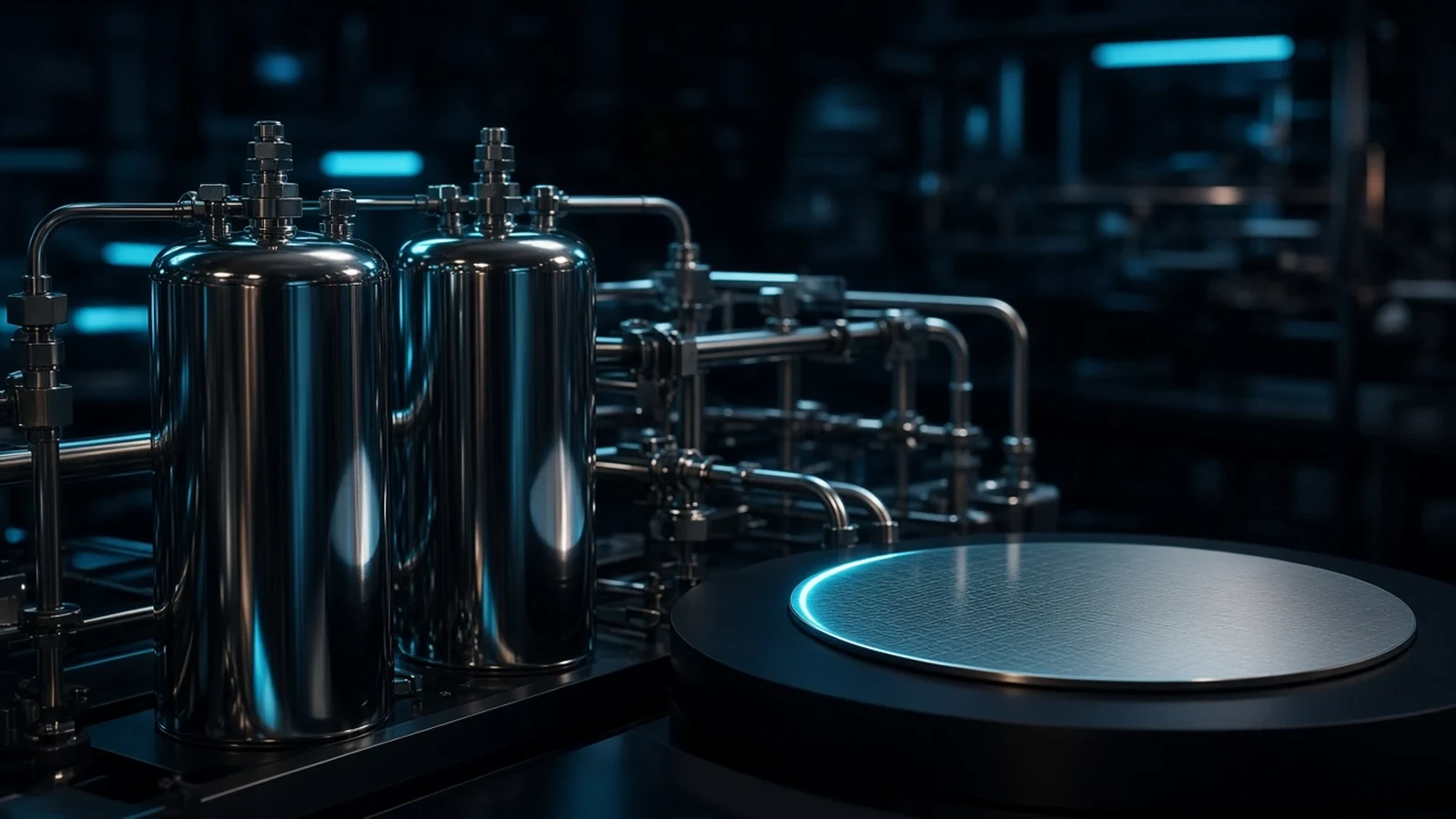
Entegris Advanced Deposition Materials is a process-materials platform for precursor and deposition chemistries used in semiconductor manufacturing.
AutomotiveAI & HPCData Center+1View Technology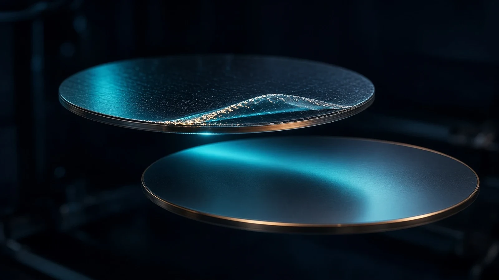
Soitec Smart Cut is the engineered-substrate process used to transfer a thin crystalline silicon film onto an insulator, producing SOI wafers.
AutomotiveIndustrialConsumer Electronics+1View Technology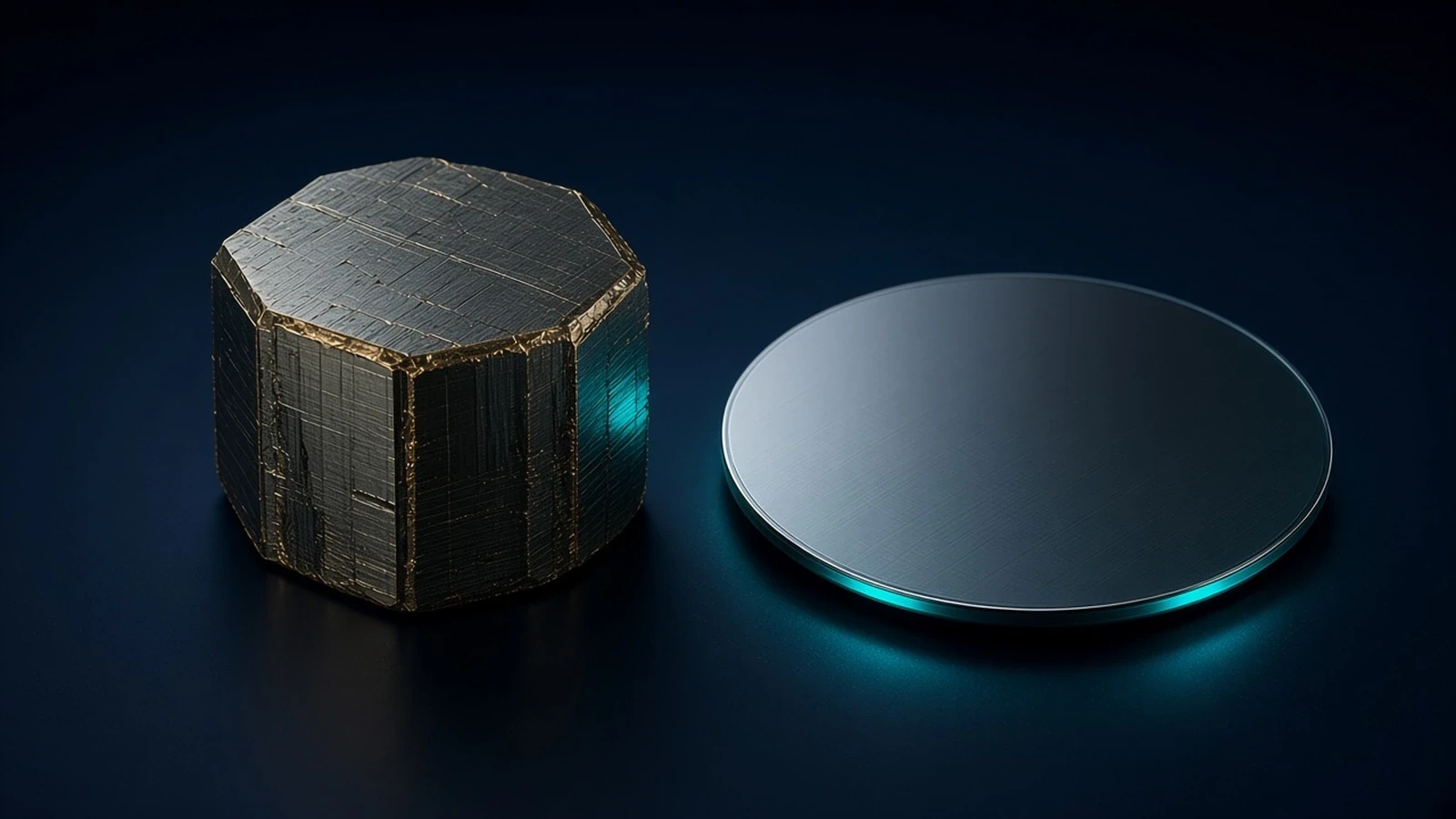
Wolfspeed conductive silicon carbide substrates and SiC epitaxy materials offered for power-electronics device manufacturing.
AutomotiveIndustrialEnergyView Technology