Discover 169 technologies from leading innovators around the world.
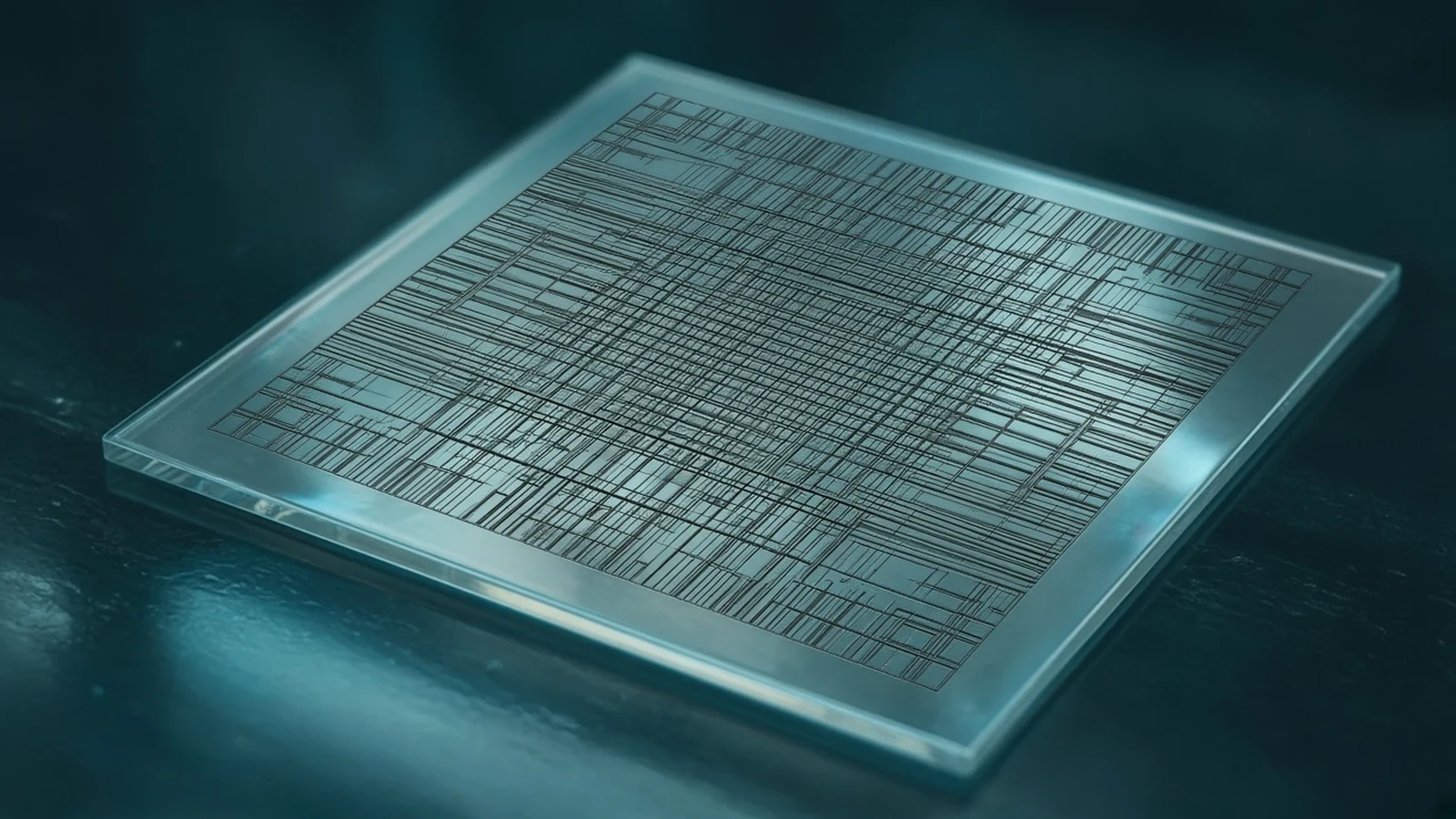
Photronics advanced IC photomasks are lithography reticles for integrated circuits, not a foundry node and not FPD masks.
AutomotiveAI & HPC+1View Technology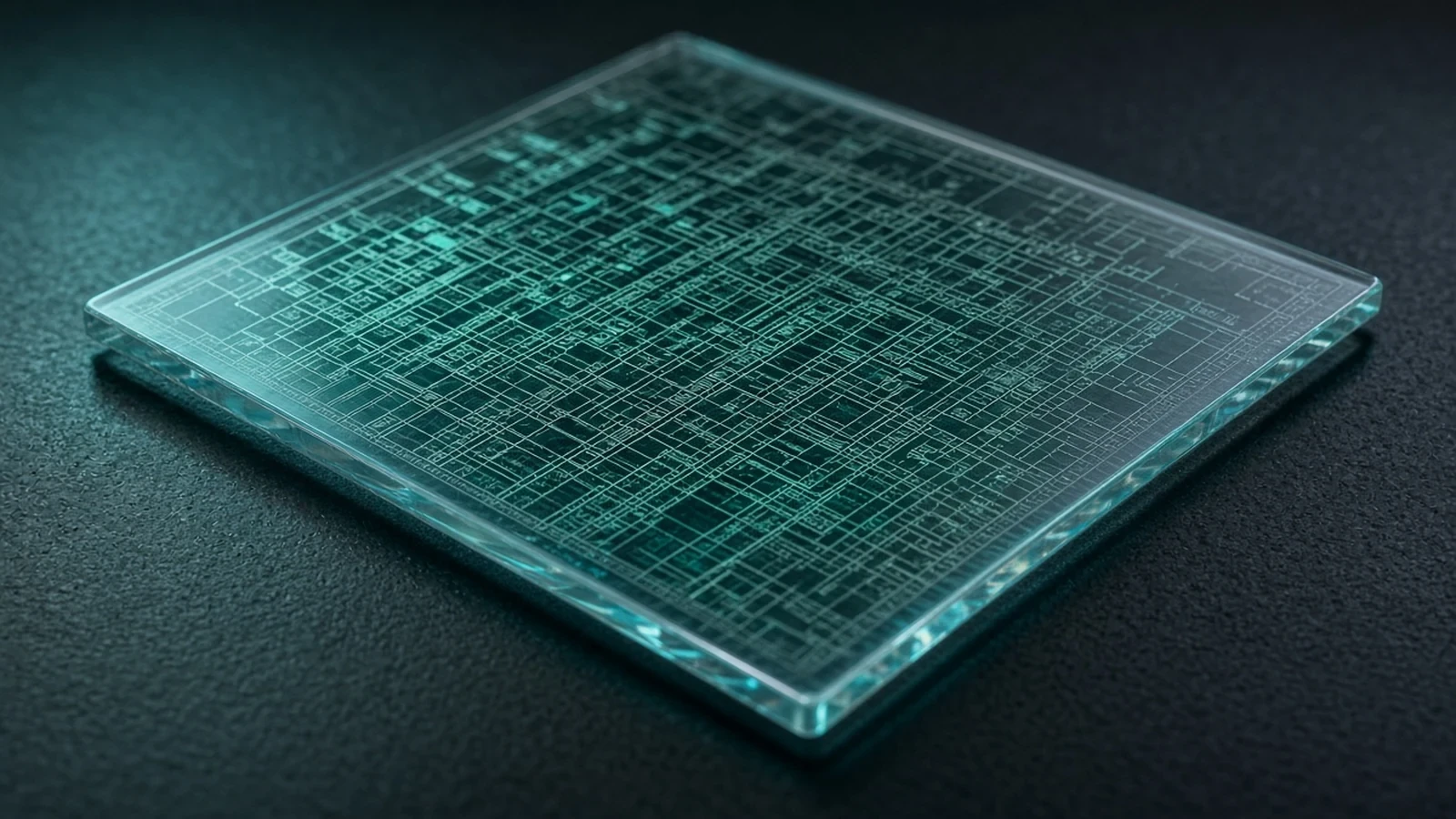
Tekscend semiconductor photomasks are lithography reticles, not a foundry process node and not a mask writer.
AutomotiveAI & HPC+1View Technology
Qnity Emblem is a next-generation CMP pad platform for advanced-node planarization, not a polishing tool.
AI & HPCData Center+1View Technology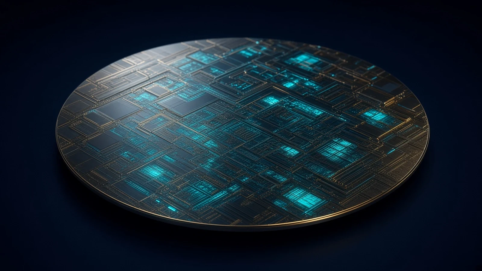
GlobalWafers Silicon Wafers are the company's silicon starting substrates, including annealed, epitaxial, SOI and diffusion wafers.
AutomotiveAI & HPC+2View Technology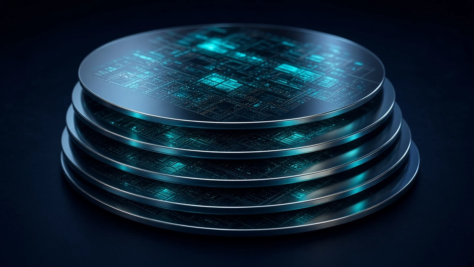
SUMCO Advanced Silicon Wafers are polished and specialty silicon starting substrates, including epitaxial, annealed and SOI wafers.
AutomotiveAI & HPC+2View Technology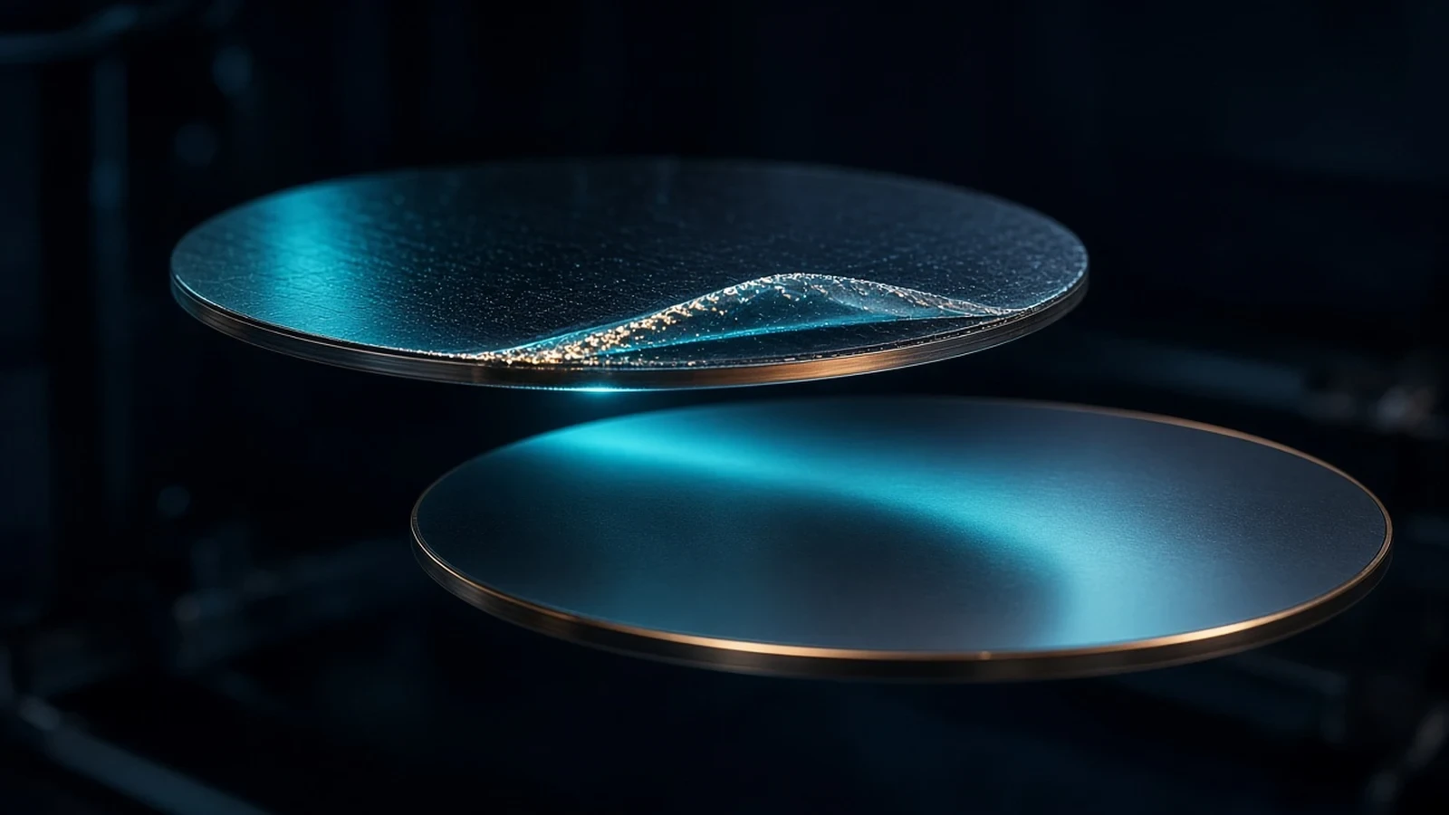
Soitec Smart Cut is the engineered-substrate process used to transfer a thin crystalline silicon film onto an insulator, producing SOI wafers.
AutomotiveIndustrial+2View Technology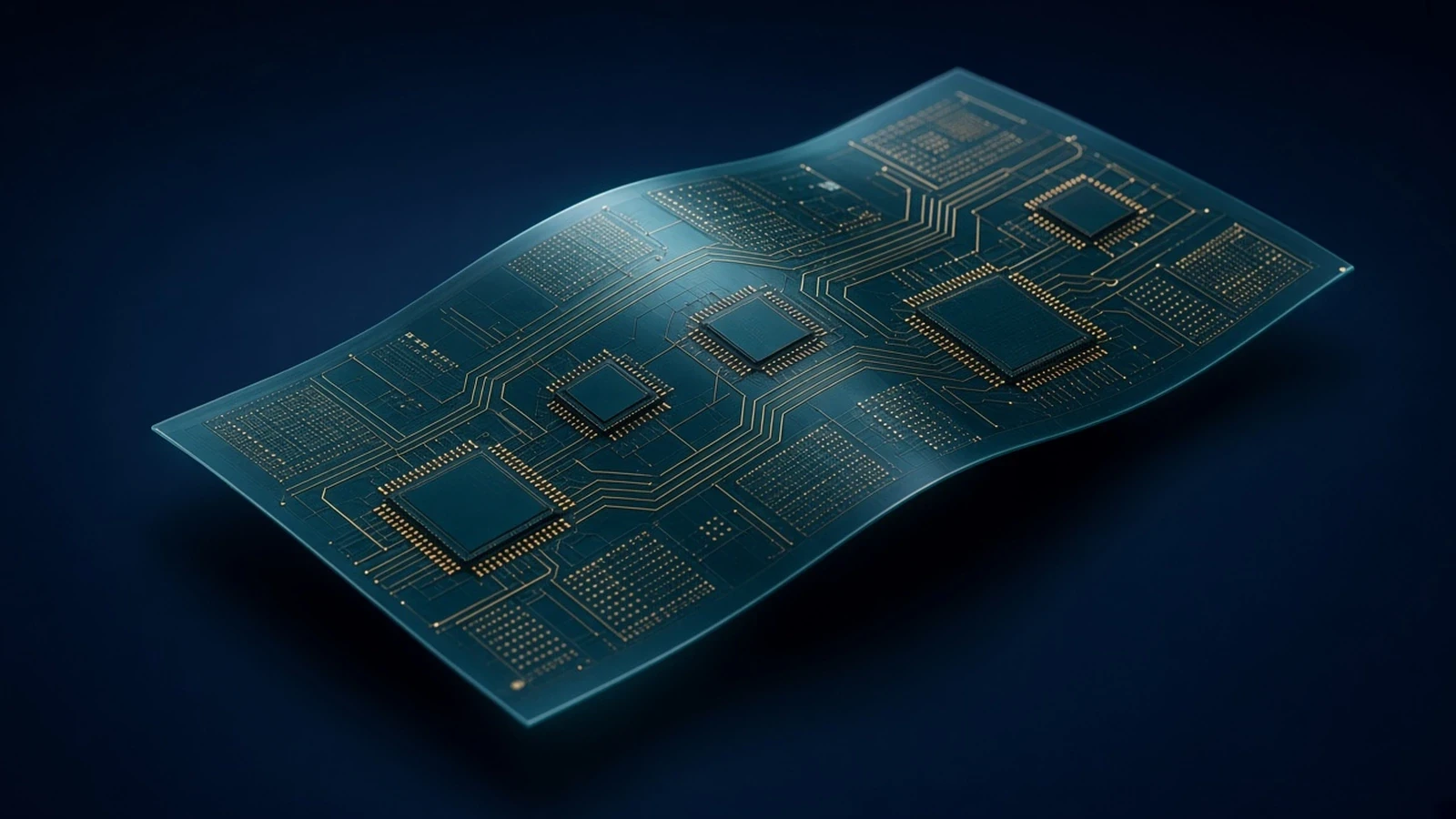
Pragmatic FlexIC Platform Gen 3 is a flexible semiconductor technology platform using metal-oxide thin-film transistors on flexible substrates for mixed-signal integrated circuits supporting connect, sense and basic compute functions.
IndustrialConsumer Electronics+1View Technology